m/matl Technology File Editor – New Release

[two-thirds]

A new release of the m/matl EM Technology File Editor is now available.

New features:

  • Import of technology information from Cadence Assura procfiles
  • Export to Empire XCcell 3D EM
  • Export to Asitic tek file (beta)

For more information and download, click here.

Import from Cadence Assura procfiles

You can import substrate information from existing Cadence Assura procfiles.

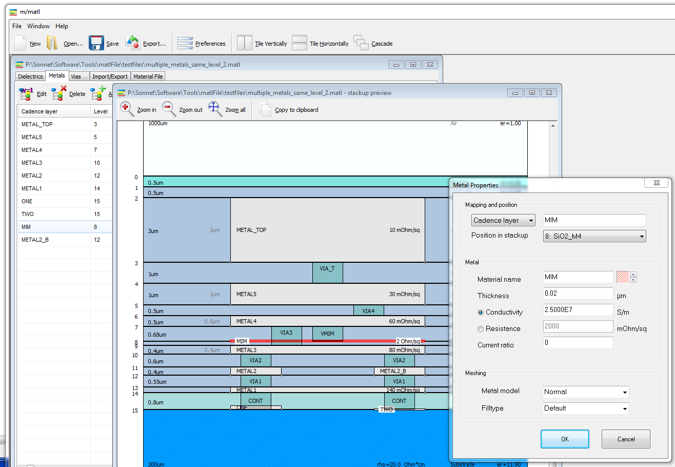
To use this option, use File > Import and select an Assura procfile. The software will evaluate the procfile, and also try to find and evaluate two additional files in the same directory: p2lvsfile and lvsfile. If these additional files are not available, the via information is missing and you need to set the via layout (from… to …) manually.

Unfortunatly, the layer names used in the Assura files do not always agree with the layer names used in the layout editor. During import, m/matl tries to figure out the layer names, as best as it can. Sometimes, this is not possible and you need to set the correct Cadence layer names manually.

Important limitations for using Assura procfile import:

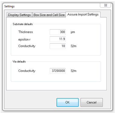
It is important to understand that the substrate itself is not included in any of these files. The substrate thickness, permittivity and conductivity are added based on m/matl default values. These default values can be set with File > Preference > Assura Import Settings.

In this dialog, there is also a settings for via conductivity. The via conductivity might be defined in the Assura files, or it might be missing. If the information is missing, the default will be used and this default assigment is listed in the import summary message.

Another note in the import summary message is related to the deposition steps. At the surface of the substrate, there are multiple deposition steps 1 defined, for different areas of the chip. The m/matl import uses only the first line for deposition step 1, which is usually for field oxide, and skips the other deposition step 1 entries. These skipped lines are listed in the import summary message.

For metal sheet resistance specified in the p2lvsfile as (Ri,wi) pairs for width dependent sheet resistance, m/matl uses the last entry, which is supposed to be valid for widest metal traces.[1]

Carefully check your results! The Assura import has been tested and optimized with many different design kits. However, there is some “educated guess” required in some cases, especially for layer names. If you experience problems, please let us know!

[/two-thirds]

[third]   [/third]


[1] From the Assura documentation: “Additionally, the (ri,wi) pairs should be specified in order of increasing width.”

Sonnet Verification Kit for TowerJazz SBC18H


[two-thirds]

Dr. Mühlhaus Consulting & Software GmbH has now released Sonnet Verification Kit for TowerJazz SBC18H

This new Sonnet verification kit is designed for simulation of passive components such as inductors and transformers in the TowerJazz SBC18H process family including SBC18HA, SBC18HX, SBC18H2 and SBC18H3 amongst others. The definitions for the Sonnet model file of conductivity, permittivity, dielectric and conductor thicknesses are current with the TowerJazz Process Specification NPB-PS-0267 rev17.

The Sonnet files apply to all SBC18H processes with 2.81um thick Al top metal and identical interconnect stackup as SBC18HX. The S-parameter measurements and GDSII layout data for the inductors used in this work were provided by TowerJazz.

The Sonnet Verification Kit is available to TowerJazz customers from the TowerJazz eBizz website, section “Special Tools”.

[/two-thirds]

[third]    [/third]


EMPIRE XCcel 6.00: New Thermal Solver

New Thermal Solver

[two-thirds]

With its new release, the well‐known 3D EM solver EMPIRE XCcel now features a novel thermal solver for the simulation of the temperature distribution of power electronics, RF circuits, integrated circuits and also including electromagnetic heating in human bodies.

The thermal simulation includes thermal conductivities of materials, surface convection and radiation cooling and supports heat sources and heat sinks for heating and cooling mechanisms.

With increasing packaging density of RF circuits heating can become a severe problem for the lifetime of critical components such as diodes (also LEDs), transistors, resistors, and ICs. Also passive structures such as filters, couplers or resonators can exhibit high currents in small areas where the temperature can rise to a critical level. In case of electromagnetic radiation the prediction of thermal heating inside of human bodies (e.g. handheld antenna attached to human head) is necessary to prevent hazards.

Figure 1: LTCC module with LEDs and driver circuit (click to view full size)

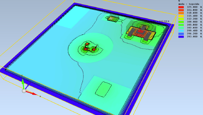
Figure 2: Temperature distribution on the LTCC module (click to view full size)

The accurate prediction of the temperature distribution is now possible with EMPIRE XCcel 6.00. The structure is created within the GUI where properties such as thermal conductivity and heat transfer rates can be entered similar as the electromagnetic properties. A large database is already equipped with known parameters. Thermal sources can be set directly, e.g. by entering a thermal power in Watt for a lumped element such a transistor. Thermal sources can be determined by an EM simulation, too. With a combined EM and Thermal simulation the RF losses are calculated in a first EM simulation run and will be used as a source for a subsequent thermal simulation. Cooling elements can be defined as surfaces with a specific thermal resistivity. In case of human body thermal modeling also the blood perfusion rate can be taken into account. In addition, known thermal properties are available in a tissue data base.

The simulation engine automatically identifies the surface to air interfaces and invokes the heat transfer mechanisms such as radiation and convection. With this method, cells filled with air don’t need to be part of the solution thus minimizing the number of cells to be simulated for the temperature distribution. A robust and efficient solver kernel is used for the fast solution of the thermal equations. An adaptive scheme optimizes the over‐relaxation factor during the iteration process for maximum simulation speed. After simulation the temperature distribution can be displayed together with the structure. The temperature can be displayed as distinct planes, as maximum or minimum of each plane or as top‐ and bottom side temperature distribution. The latter is especially intended for the comparison with infrared camera pictures.

As an application example an LTCC module is shown in Figure 1 which has been developed in a joint project of the German companies odelo LED GmbH, IGOS GmbH and IMST GmbH and was co‐funded by the German federal state North Rhine Westphalia (NRW) and the European Union (European Regional Development Fund: Investing In Your Future). It contains 3 LED chips on top which are die‐ and wire‐bonded to the top metallization. A small driver circuit with Shottky diode, transistor and resistor is placed on top side, too. Many thermal vias are integrated beneath the active elements to transfer the heat from the topside to the heatsink at the bottom side. In this case the power loss is known and entered as lumped and distributed heat sources.

Figure 2 shows the topside temperature distribution obtained with EMPIRE XCcel 6.00. The module is subdivided into 10.3 million cells and an accuracy of 0.6 mK has been obtained after 2700 iterations. The simulation time needed is about 3 minutes on a Notebook with Intel Core i7‐2620M CPU @ 2.7 GHz. For this size the memory requirement is about 1 GByte. The temperature rise is about 40 K above ambient temperature with the maximum inside the transistor package.

As can be seen a temperature distribution for a complex structure is obtained with EMPIRE XCcel 6.00 which gives valuable input for the thermal design. As known from EMPIRE XCcel’s unique fast FDTD kernel, the new thermal solver has also been optimized with respect to solution speed thus giving reliable results within minimum of solution time.

[/two-thirds]

[third] [/third]

3D EM Solver: Empire XCcell 6.0 released

“Faster on CPUs than others on GPUs”

[two-thirds]On market since 1998, EMPIRE has always been the first choice for EM design of complex structures. IMST has now released the new version 6.00, which is even further optimized to solve huge structures, hundreds of wavelength in size.
[/two-thirds]
[third] [/third]
[divider]

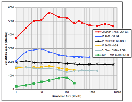
New speed records:

  • Cluster solver: 11200 MCells/s on 7 Intel Core i7-3960 (up to 7 x 32 GByte)
  • Single PC solver: 5600 MCells/s on Dual Intel Xeon E2690 (up to 512 GByte)
  • Single PC solver, SSD swapping: 1800 MCells/s on Intel Core i7-3960 (up to 1 TB)

New features include:

  • Thermal solver including heat sources, RF losses, conductivity, convection, radiation
  • Poser for human body models
  • High speed simulation on Solid State Disks (SSD)
  • Additional Optimizer algorithms (Global Direct, Nelder Mead, MSLS)
  • Optimization on single value goals (e.g. beamwidth, efficiency)
  • Human body thermal effects of EM radiation
  • Postprocessing (e.g. far field transformation) on remote servers
  • Field monitors for volumes, planes, paths, probes
  • Smooth display of fields on complex surfaces
  • Parameter sweep mapping to formulas or lists
  • Arbitrary oriented (off-axis) lumped ports
  • Active impedance simulation (simultaneous excitation of unequally numbered ports)
  • Enhanced field display features, e.g. markers in animations

To use the new modules (Thermal Solver, Poser), a separate license feature is required.

For more information about Empire XCcell, see the product page.
30 day evaluation versions are available, please contact us for more details.

[divider]

Application Examples

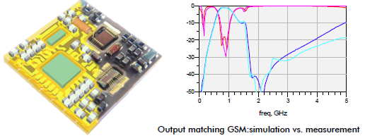
Complete HPA module for GSM and XCS

  • Simulation time: 1 min
  • Memory usage: 150 MB,
  • Size: 3 MCells
  • Dual Xeon E2690
  • DC – 5 GHz
[divider]

KA Band TX waveguide aperture radiating 32 x 32 antenna array


  • Simulation time: 8 min
  • Memory usage: 3.6 GB,
  • Size: 87 MCells
  • Dual Xeon E2690
  • 29.5 GHz

Sonnet 13.56: Skill Scripts for Cadence Design Flow

New utilities for Cadence design flow

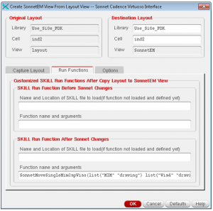
In Sonnet 13.56, some new utilities have been added to support the Cadence<>Sonnet design flow. These are implemented as Skill scripts and can be customized by the user if needed.

This functionality is added by the new Skill scripts:

  • Remove unwanted polygons from SonnetEM, based on layer purpose
  • “Stop via” implementation as used for MIM-capacitors and resistors
  • Merge a meshed ground plane into a solid polygon, with cutouts for vias

All these scripts are explained in detail below.

Introduction

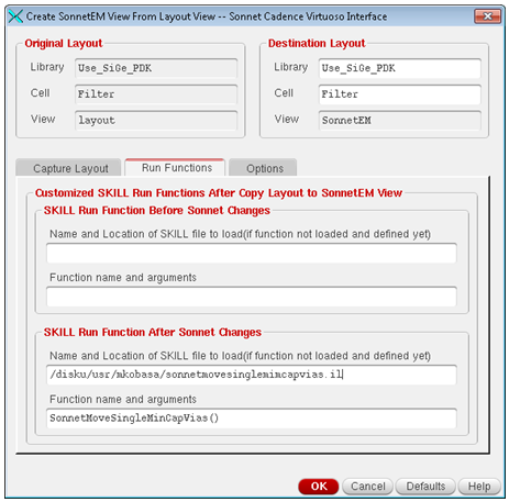
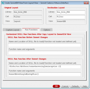
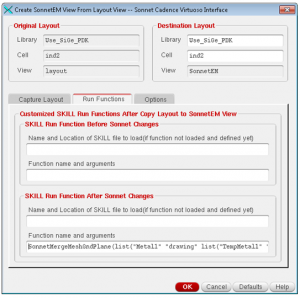
When creating the Sonnet EM view from the Caddence layout view, the Sonnet interface can run pre- and postprocessing scripts. This enables customized modification of the layout, to prepare it for efficient EM simulation.

(click to view full size)

[divider]

Remove unwanted polygons based on layer purpose


[half]

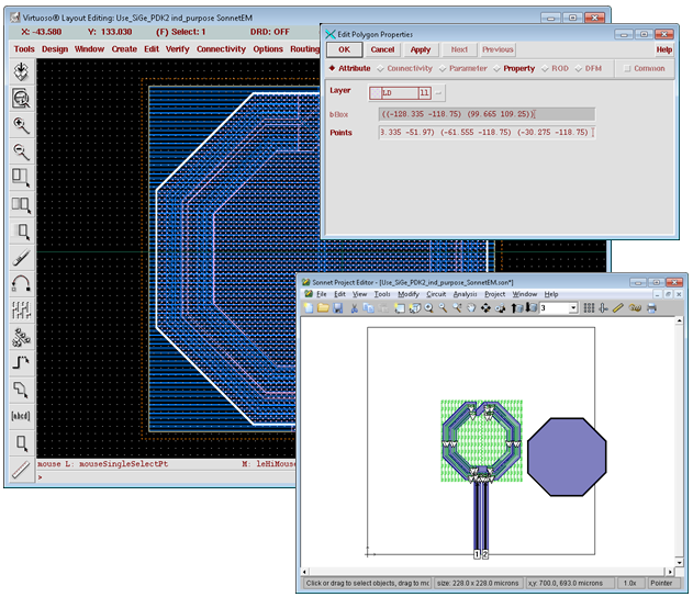
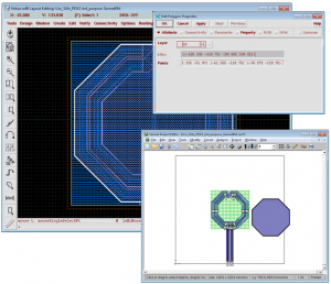
Some designs in certain PDK’s for parasitic extraction have polygons on a non-drawing purpose such as the “ll” purpose. Without using the new script, the layer mapping from Cadence to Sonnet does not evaluate the purpose, so designers would have to delete these extra polygons manually.

In the picture below, the unwanted polygon is moved in the Sonnet editor, to show this extra polygon better.

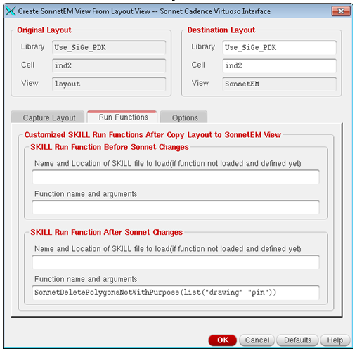
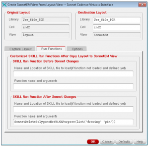
In Sonnet 13.56, we have a new script to remove these extra polygons. The default is to keep polygons on the “drawing” purpose and the “pin” purpose. Deleting polygons only happens in the SonnetEM view and not in the original layout.

You can easily run this script when creating the SonnetEM view and pass in a list of purposes to keep.

SonnetDeletePolygonsNotWithPurpose(list("drawing" "pin"))
SonnetDeletePolygonsNotWithPurpose()

[/half]

[half]

(click to view full size)[/half]


[divider]

Stop via implementation


[half]

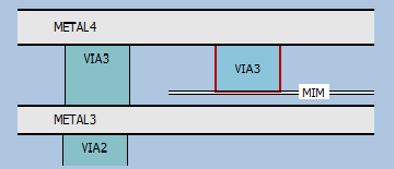
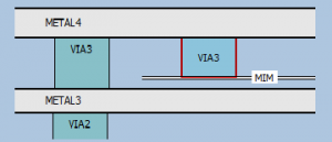
In some technologies, the same via layer is user to connect to different metal layers. This is sometimes found in MIM capacitors or resistors. In the example below, you can see that VIA3 connects to Metal3 or MIM, depending on the presence of the MIM metal layer.

In Sonnet 13.56, we have a new script to handle this situation.

This simple script will move the polygons on the via drawing layer connecting to the MIM layer to a temporary drawing layer for translation purposes. In the Cadence to Sonnet layer mapping , we can then use that new via to connect to the MIM layer.

Of course, moving of polygons only happens in the SonnetEM view and not in the original layout.

You can easily run this script when creating the SonnetEM view and pass in the appropriate layer purpose pairs. Syntax is to pass in the layer purpose pair (LPP) of the MIM layer, then the via LPP connecting to the MIM and finally the new temporary via LPP

IMPORTANT: When using the script, the .matl file needs to be edited so that the new temporary drawing layers used are mapped properly.

[/half]

[half]

(click to view full size)[/half]
SonnetMoveSingleMimCapVias(list(“MIM” “drawing”) list(“Via3” “drawing”) list(“TempVia3” “drawing”))

[divider]

Simplify meshed ground plane


[half]

Due to layout rules, large ground planes are often implemented by a mesh of lines, instead of a filled area. Electrically, this mesh will behave very similar to a filled area. The filled area representation is much more efficient for EM simulation. By using a new script, we can now convert the meshed area to a filled area, for much faster simulation.

This new script will simplify a ground plane, but leave the required keep out areas for pins and vias.

Technically, this script will grow all of the metal on certain drawing layers, merge them all together and then shrink all of the metal back to its original size. Merging of polygons only happens in the SonnetEM view and not in the original layout. You can easily run this script when creating the SonnetEM view and pass in the appropriate layer purpose pairs.

Syntax is to pass in the layer purpose pair (LPP) of the ground layer which you want to merge and then a LPP that is used to temporarily move the polygons to in the algorithm.[/half]

[half]
(click to view full size)[/half]

SonnetMergeMeshGndPlane(list(“Metal1” “drawing”) list(“TempMetal1” “drawing”))

[divider]

Installing the new scripts

The Skill scripts are located in <SONNET_DIR>/sonnet_virtuoso_dk/skillutil.

It’s best to install these scripts after the interface is installed in the .cdsinit file so that they are easily available for use. Just load in the .il files that you might be interested in using and the parameters can be passed into each function when creating the SonnetEM view.

aSonnetDir = getShellEnvVar("SONNET_DIR") 
;// Loads the Sonnet Move Single MIM Cap Vias Utility
loadi(simplifyFilename(strcat(aSonnetDir "/sonnet_virtuoso_dk/skillutil/sonnetmovesinglemimcapvias.il"))) 
;// Loads the Sonnet Move Dual MIM Cap Vias Utility
loadi(simplifyFilename(strcat(aSonnetDir "/sonnet_virtuoso_dk/skillutil/sonnetmovedualmimcapvias.il"))) 
;// Loads the Sonnet Move Resistor Vias Utility
loadi(simplifyFilename(strcat(aSonnetDir "/sonnet_virtuoso_dk/skillutil/sonnetmoveresistorvias.il"))) 
;// Loads the Sonnet Delete Polygons Not With Purpose Utility
loadi(simplifyFilename(strcat(aSonnetDir "/sonnet_virtuoso_dk/skillutil/sonnetdeletepolygonsnotwithpurpose.il"))) 
;// Loads the Sonnet Mesh Ground Plane Utility
loadi(simplifyFilename(strcat(aSonnetDir "/sonnet_virtuoso_dk/skillutil/sonnetmergemeshgndplane.il")))

 

Sonnet 13.56 now available

Sonnet Professional 13.56

This release provides a number of changes in the Sonnet Interfaces and also contains a beta of the new Inductor Model Extractor which will be introduced in release 14 of Sonnet. Please see below for details.


Compatibility with ADS 2011

[half]

Sonnet’s Agilent ADS Interface now supports Agilent’s ADS 2011 version.

For information on using Sonnet’s Agilent ADS Interface with ADS 2011, please refer to the Sonnet’s Agilent ADS Interface Release 13 Update document included in your release. Select Help > Manuals from any Sonnet application, then click on the link for the Translators. For the most up to date compatibility requirements, please see http://www.sonnetsoftware.com/requirements.

[/half]

[half][/half]

Inductor Model Extractor beta

[half]

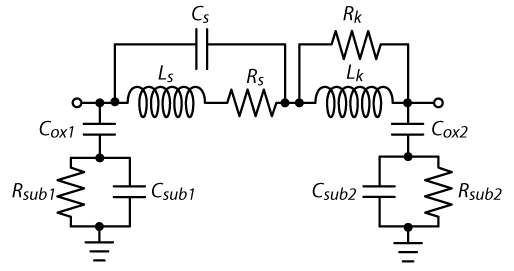
Sonnet version 13.56 introduces the beta version of a new Inductor Model Extractor feature which allows you to output an equivalent circuit model for an inductor with a “Skin Effect” topology. The inductor model may be output as a Spectre or PSpice data file, or a Sonnet netlist. You may set up this output before analysis in the project editor or create the file in the response viewer after your analysis is complete.

For more information on enabling and using this beta feature, please see the documentation available on our web site at http://www.sonnetsoftware.com/beta.

[/half]

[half][/half]

[half]

Enhanced Cadence Interface

For information on the changes in Sonnet’s Cadence Virtuoso Interface, please see the Sonnet’s Cadence Virtuoso Interface Release 13 Update document included in your release. Select Help > Manuals from any Sonnet application, then click on the link for the Translators.

Bug fixes and known bugs

Check the Sonnet web site for the latest information and the most up to date list of known bugs and bug fixes: http://www.sonnetsoftware.com/release-notes

[/half]

[half]

Updated  .matl file documentation

This release includes an updated documentation of the Sonnet process file (.matl) format to add missing entries and correct mistakes in the .matl File Format appendix in the release 13 Translators manual.

The information in the .matl File Format document supersedes the information in the appendix. Select Help > Manuals from any Sonnet application, then click on the link for the Translators to access this document.

[/half]


[half][box type=info]Sonnet 13.56 download information[/box][/half]

[half][box type=info]What’s new in Sonnet 13.56[/box][/half]


New Version of m/matl EM Technology File Editor

We have released a major update for the m/matl EM Technology File Editor.

New and updated in the 25. Jan 2012 release:

  • Major new revision with new user interface and new functionality
  • Support for multiple metals on the same level, with proper visualization
  • Import *.son model
  • Export *.son model for stand alone use
  • Manage and export layer mappings for GDSII and DXF workflow,
    to enable multi-design-flow support from a single source file
  • Many details updated for better improved usability
  • User’s Guide in PDF format included

https://muehlhaus.com/material-file-utility

New application note: Stacked Metal

Stacked Metal in Sonnet Inductor Models

[two-thirds]

The purpose of this document is to assist you with simulation of inductors that have stacked metal, connected by large via array.

via meshing

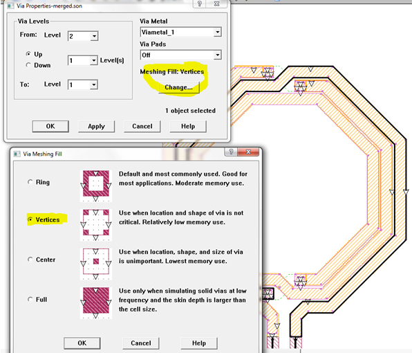
Often, these via arrays cover the entire conductor area, making the analysis slow and take much memory. We will investigate the physical behaviour of the via array at high frequency, and derive better modelling techniques that are more efficient in terms of simulation time and memory.

[box type=info]RFIC Stacked Metal in Sonnet (PDF, 892kB)[/box]

[/two-thirds] [third] [/third]


New application note: Inductor Measured vs. Simulated

RFIC Inductor Measured vs. Simulated Troubleshooting

[two-thirds] The purpose of this document is to assist you with resolving possible differences between simulated RFIC inductor results and values obtained from the design kit or from measurement.

Inductor lumped model

This document is based on extensive practical experience. The author has worked for many years in RFIC inductor modelling, and worked closely with the modelling and measurement groups of different foundries.

[box type=info]RFIC Inductor Measured vs Simulated (PDF, 540kB)[/box]

Updated 31. Jan 2012:
Added description how to calculate differential L and differential Q
from 2-port and 3-port simulations. Below is the Sonnet equation file.

[box type=info]Differential inductor equations Ldiff and Qdiff (ZIP, 1kB) [/box]

[/two-thirds][third] [/third]