m/matl – The EM Technology File Editor for RFIC
[two-thirds]Our EM technology file editor m/matl simplifies the setup of complex EM stackups for RFIC/MMIC technologies. From a single stackup definition, you can create substrate files for different popular EM workflows, as well as cross section pictures and material settings tables for documentation.
The tool is available to Mühlhaus Consulting & Software GmbH customers at no extra cost.
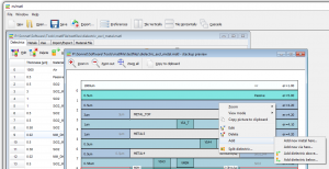
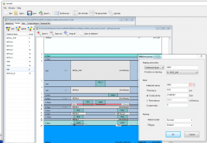
m/matl – cross section view (click for full size)
- semi-proportional view (click for full size)
[/two-thirds] [third] [/third]
[two-thirds]m/matl helps you to create EM substrate files for popular EM workflows, like Sonnet EM and Agilent ADS Momentum. You can define stackups starting from an empty file, or import existing files from Sonnet *.matl, Sonnet *.son, Agilent *.slm, Agilent *.subst or Cadence Assura procfiles.
The stackup can be visually inspected in different views. Material data input can be specified and displayed as thickness & conductivity, or as thickness & ohm/square which is typically specified in foundry data sheets.
To simplify the stackup and prepare it for more efficient EM simulation, dielectric layers can be merged, creating a new dielectric with the total height and the effective epsilon, or splitted into multiple pieces.[/two-thirds] [third] [/third]
[two-thirds][box type=info]Current version: 27. March 2013
m/matl version 27. March 2013 (zip, 1.8MB)[/box][/two-thirds] [third] [/third]
[divider]
File formats:
| Read | Write | Used for | ||
| Sonnet *.matl | X | X | Sonnet interfaces to Cadence and ADS | |
| Also used as primary m/matl file format | ||||
| Sonnet 12 *.son | (X) | X | Sonnet stand alone | |
| Sonnet 13 *.son | (X) | X | Sonnet stand alone | |
| Sonnet *.lay | – | X | Sonnet GDSII workflow | |
| Sonnet *.lyr | – | X | Sonnet DXF workflow | |
| ADS 2009 *.slm | X | – | Momentum in ADS 2009 and earlier | |
| ADS 2011 *.subst | X | X | Momentum and FEM in ADS 2011 and later | |
| Assura .procfile | X | – | Cadence Assura | |
| Asitic *.tek | – | (beta) | Asitic inductor tool | |
| Empire XCcell *.gym | – | (beta) | Empire XCcell 3D EM | |
| Documentation *.html | – | X | Stackup documentation tables | |
| Cross section picture | – | X | Cross section image copied to clipboard | |
| X = supported | See documentation for file format details | |||
| (X) = manual layer mapping needed | ||||
[divider]
Release history
27. March 2013
- NEW: import of Agilent ADS 2011/2012 substrate files
- NEW: export of Agilent ADS 2011/2012 substrate files
- see documentation for known limitations
11. October 2012
- NEW: import of technology information from Cadence Assura procfiles
- NEW: export to Empire XCcell 3D EM
- NEW: export to Asitic tek file (beta)
03. Mar 2012
- Correct icon size in menu and toolbar is now set automatically for Windows XP, Vista, Windows 7
20. Feb 2012
- Fixed a problem with regional settings and the decimal separator “,”
- Fixed a bug with incorrect GDSII via layer numbers for *.lay export (layer mapping file for GDSII workflow)
2. Feb 2012
- File > Export: Added html documentation output with a list of dielectrics, metals and vias
- Added calculator button for via conductivity from via resistance and dimensions
- Force “safe” layer and material names with underscore instead of space
- Better display of via from/to layer name when thick metal fills a complete dielectric layer height
25. Jan 2012
- Major new revision with new user interface and new functionality
- Support for multiple metals on the same level, with proper visualization
- Import *.son model
- Export *.son model for stand alone use
- Manage and export layer mappings for GDSII and DXF workflow,
to enable multi-design-flow support from a single source file - Many details updated for better improved usability
- User’s Guide in PDF format included
7. Nov. 2011
- Compatibility: Changed matl output format of new metal, for compatibility with Sonnet 12
4. Nov. 2011
- Drawing now side by side with material grids
- “Edit” from cross section view now brings up editor dialog, instead of switching to metal/via/dielectric tab
- Vias on adjacent layers are now aligned if they have the same layer name
- slm import: Fixed mistake with incorrect target layer for thick metal expansion down
- slm import: Fixed error with via span for thick metal, expansion down
- slm import: Fixed error with very old slm file, which did not have metal data field 11 (thin/thickup/thickdown)
10. Oct. 2011
- Metals, vias and dielectrics can now be selected from the drawing
- Highlight last selected object in drawing
9. Oct. 2011
- Vias draw after metal, so that multi-level vias are easier to identify
- Bottom of via is now drawn to top of metal on level (if any)
- Fixed number format in dielectric grid
- Fixed add above/below in context menu
- Added split dielectric feature
- Pattern for new metal/via now counts up automatically
17.Sept. 2011
- Added support for commandline paramter and file drag&drop
- slm files can now be loaded from File > Load, without having to use File > Import > SLM


