
Small ceramic antennas have become popular as they occupy less board space than traditional PCB antennas. However, the small package of those ceramic devices is only one part of the antenna: it radiates by interacting with a much larger PCB ground. Only if these pieces are properly co-designed, with sufficiently large PCB ground, we obtain the expected antenna performance.
Inexperienced designers often misinterpret the small ceramic antenna package and place it very differently from the manufacturers prototype design, on a much smaller PCB. This results in antenna impedances that are difficult to match and have poor radiation efficiency. In this simulation report, we will review the importance of placement and PCB dimensions.
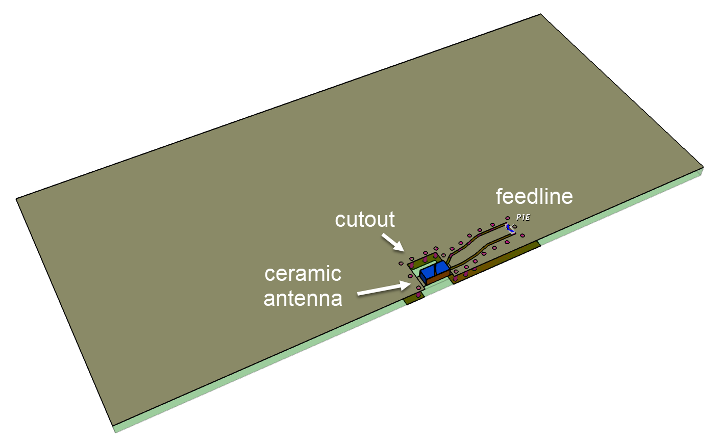
Figure 1: Ceramic antenna and cutout on middle of PCB ground plane edge
Different types of small ceramic antennas
Many small “chip” antennas are designed as shorted monopoles, with a miniaturized meander or helix on a dielectric core. These 1-port devices are typically placed on the corner of a PCB, with that corner completely cleared from any metal ground. The short monopole is then matched to 50 Ohm using discrete LC matching.
In contrast, the antenna investigated here is a 2-port device that must be complemented by a PCB conductor loop around a clearly defined cutout. The antenna is part of the loop and current is flowing around the cutout. This excitation is then radiated by the PCB metal plane.
Device under test
Device under test in this report is a Pulse Larsen W3011 GNSS antenna operating at 1575 MHz. The author of this simulation report is not affiliated with the antenna manufacturer, and only came across that device during simulation support for a client who had unsuccessfully tried it on a very small PCB, despite warnings in the data sheet. To better understand this antenna type and layout requirements, EM simulations were used for parameter studies and field visualization.
The W3011 ceramic device has 2 terminals and can be understood as a capacitor, so that by adding a PCB cutout with inductance from path length we have a resonant structure in the cutout region. With proper placement of that current loop on the edge of a large PCB, good radiation performance can be achieved. PCB ground plane is required to guiding radiation and efficiently couple the loop to free space. Only if we combine all these ingredients properly, we have a functional antenna.
To avoid misunderstanding, it must be noted that this antenna concept is not using PCB material as a dielectric resonator. Performance is unchanged if PCB top and bottom planes are connected by via fences,shorting electric field inside the PCB dielectric. It is the PCB metal plane that interacts with slot excitation and guides the waves.
Although we have a current loop operated at resonance, the antenna is not a simple “magnetic loop” antenna either, which has a radiation pattern zero perpendicular to the loop. There is more complex interaction between the resonant currents in the slot region and the metal plane. As we will see later, the pattern looks more like a dipole on the long axis of the PCB, with the resonator slot in the center.
Modelling
To study antenna behaviour with different PCB shapes and dimensions, the antenna device plus PCB was modelled in 3D EM simulation. To establish a trusted baseline model, dimensions and metalization were obtained from the data sheet, leaving the ceramic material properties as the only unknown. Carefully replicating the reference PCB from the data sheet, permittivity of 87.3 was obtained by fitting simulated and measured resonance frequency. Ceramic loss tangent was set to zero in this model because conductor loss is the dominant effect on this resonator.
Impedance, bandwidth and patterns were then compared to measurement from the data sheet, and found to be on very good agreement. Now that trust in this modelling method was established for the reference layout (baseline simulation), different parameter studies were carried out.
Frequency tweaked by cutout size
Resonance frequency is determined by device capacitance between the two terminals and inductance formed by path length around the cutout. This resonator coupled to the input port masks possible resonances caused by the PCB size.
It might be unexpected to explain and treat the ceramic “antenna device” as a capacitor, but it’s really about generating a resonance around the slot, and the ceramic device provides the required capacitance between the two terminals that resonates with the inductance from path length around the cutout. Figure 2 shows the resulting current density in the slot region at resonance.
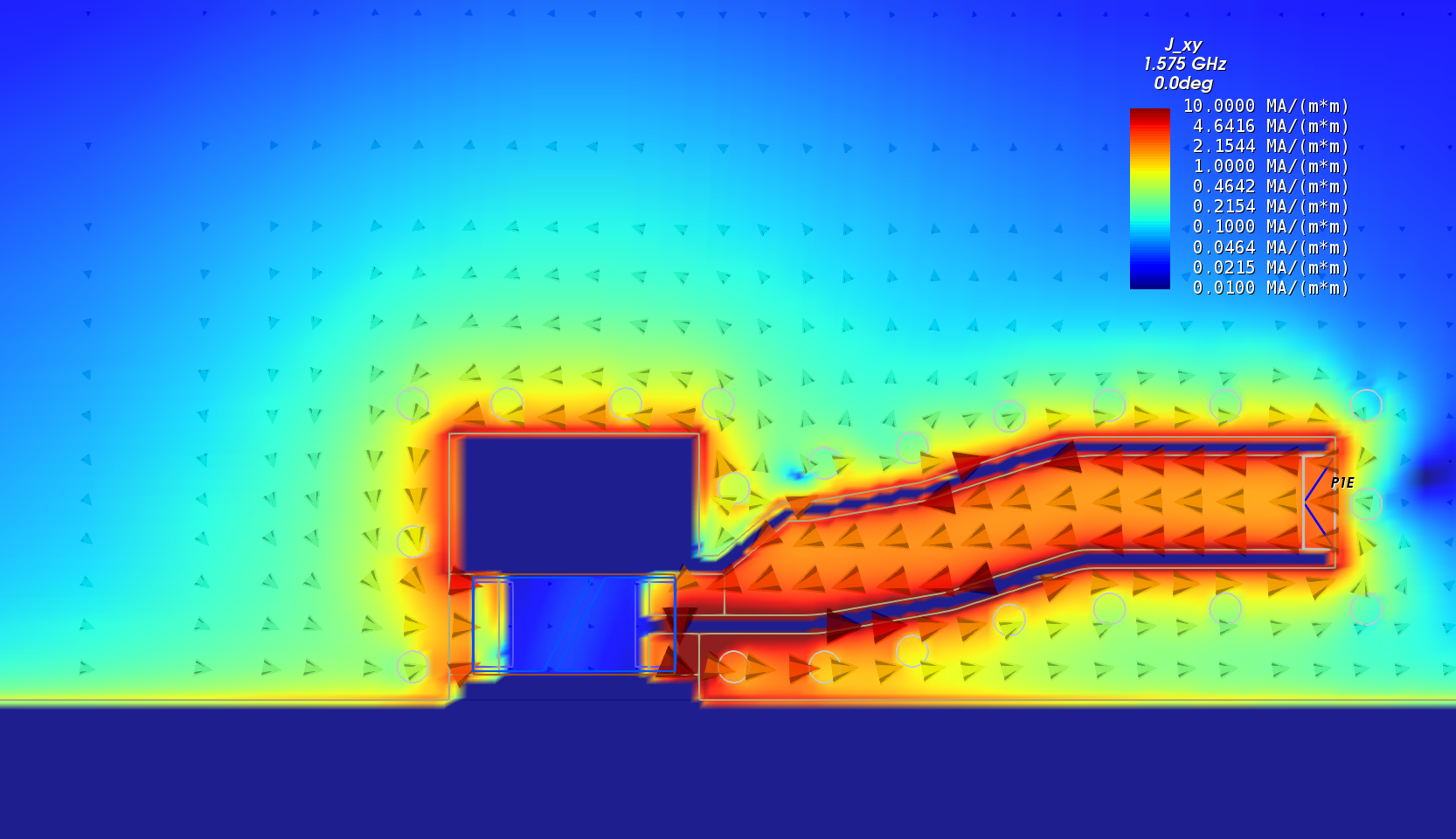
Figure 2: Current density in cutout region at resonance on top metal layer
Surrounding PCB metal is excited by this resonance, guides the signal and couples it to free space. Figure 3 shows the electric field around the 80mm x 37mm PCB at resonance.
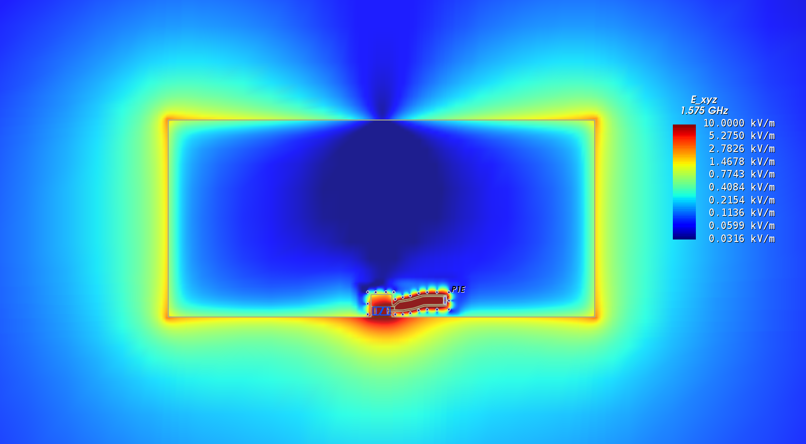
Figure 3: Electric field at resonance, measured half way between top and bottom layer
To set resonance frequency for the given ceramic device, path length around the cutout must be tweaked, to change effective inductance. Figure 4 shows the shift in antenna resonance when the nominal 4.25mm cutout length is tweaked by +/- 0.5mm, at constant cutout with of 4mm.
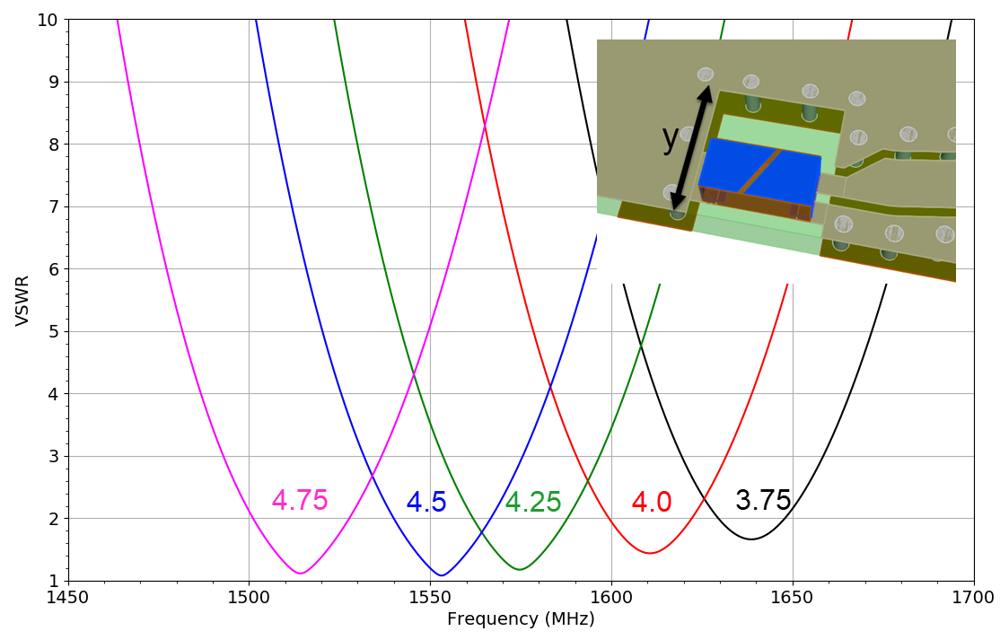
Figure 4: Resonance shift caused by tweaking the cutout size
Influence of PCB ground plane size
PCB length has only limited effect on resonance frequency at the antenna port, but a massive effect on impedance. For the model discussed here, best matching is achieved around 80mm edge length, which is approximately ½ wavelength. Smaller PCB length results in larger input resistance at resonance, and this is what broke the client’s design: his PCB was much too small, resulting in an extreme input impedance that could not be matched efficiently.
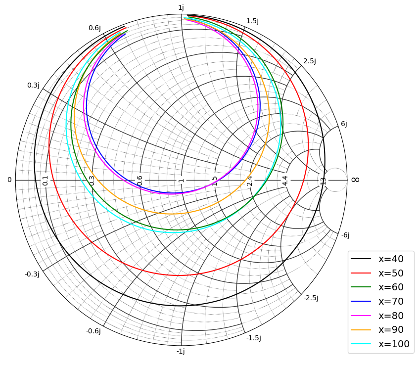
Figure 5: Impedance into antenna at different PCB length
As mentioned before, resonance frequency measured into the antenna port is not sensitive to PCB length. It only changes a few MHz or less, because the resonator from ceramic capacitance + cutout path inductance masks possible resonances from PCB conductor dimensions.
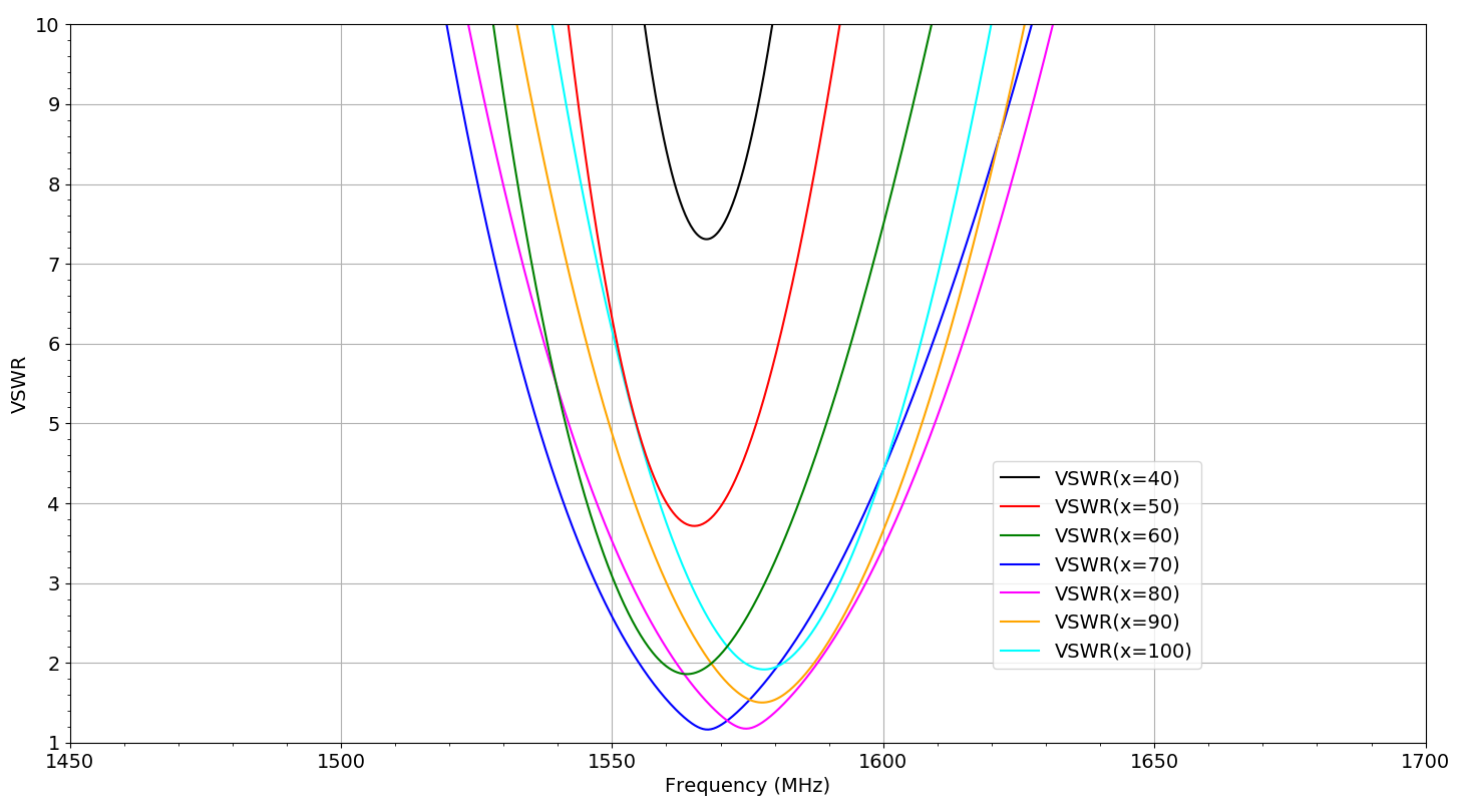
Figure 6: VSWR into antenna at different PCB length
Radiation efficiency is >90% in simulation for all simulated PCB length from 40mm to 100mm. However, antenna pattern changes: for small PCB length, antenna pattern is almost omnidirectional with no deep minima. When PCB length increases to 80mm, which is approximately half wavelength, the pattern becomes more directional, as shown in figure 7.
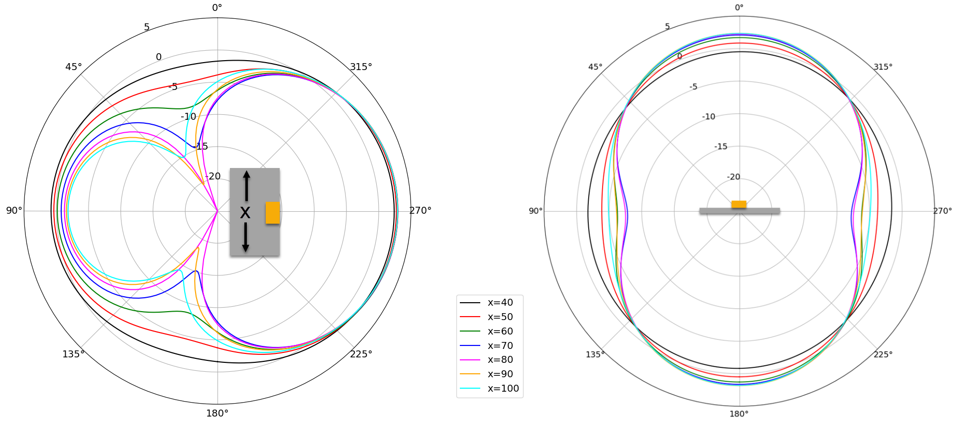
Figure 7: Antenna gain at different PCB length for width = 37mm, absolute value over all polarisations, left: azimuth sweep in PCB plane at theta=90°, right: elevation sweep at phi=0°
If we keep that 80mm PCB length but reduce width from 37mm to 8mm, resulting in a long narrow PCB shape, antenna shape and antenna pattern are coming close a dipole. Only the feed is different from a normal dipole: instead of two isolated dipole arms, we have one long conductor with the resonator in the middle, generating electric field across the cutout.
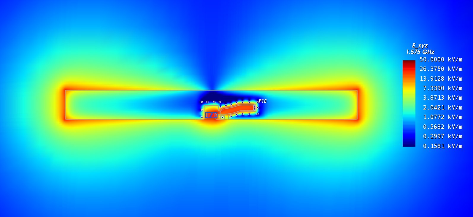
Figure 8: Electric field at resonance for narrow PCB, measured half way between top and bottom layer

Figure 9: Azimuth pattern for narrow PCB, 8mm wide x 80mm long
The narrow “dipole like” PCB version is more wideband: -6dB bandwidth is 160MHz for the narrow 8mm x 80mm PCB and 40 MHz for the wide 37mm x 80mm PCB.
Antenna feed and shunt inductance
The two terminal antenna device is symmetric regarding pads. One pad is connected to ground, the other pad requires two connections: signal input and a shunt path to ground. This shunt stub connection is the magic to achieve 50 Ohm matching at resonance, and layout is very sensitive in this region. Small shunt inductance changes of +/- 0.2 nH have a significant impact on input impedance.

Figure 10: layout details at antenna feed
The overall configuration can also be understood as a resonator with tapped inductance, where the antenna input is at the tap.
When migrating the antenna design to another PCB size, impedance matching must be adjusted, as discussed below.
Antenna on short edge
When the antenna position is moved from the middle of the long edge (80mm) to the middle of the short edge (37mm), this has a strong effect on input impedance at resonance. This is expected because we already interpreted the antenna as sort of dipole along the PCB edge, and by moving the antenna to the short edge we shorten that dipole.
Mismatch for placement on the small edge of the 37mm x 80mm PCB is almost the same as for 37mm x 37mm. What really matters is PCB length on that edge where the antenna is placed.
We can assume that the 80mm PCB length in the reference design was chosen with care: it is approximately ½ wavelength. From simulation results, a range of 50mm to 100mm seems possible if impedance matching is tweaked.
Very different PCB shape
If we change the PCB to a very different shape, input resonance frequency is still determined by the ceramic device and cutout inductance, but coupling to free space through the PCB metal might be less efficient, resulting in impedances that are difficult to match and result in less usuable bandwidth.
Ceramic antenna or capacitor?
If the ceramic antenna two-port device acts as a capacitor, does that mean we can use a regular SMD capacitor? The simple answer is yes, from simulations we get very similar antenna results when using a 1.8pF capacitor in 0805 package. However, possibly issues like tolerances and temperature drift need to be considered.
Summary
The ceramic antenna solution investigated here, based on design by Pulse Larse, is somewhat special because it enables antennas with very little cutout/keepout area on the middle of a PCB edge. This is different from other small ceramic antennas that usually operate as shortened monopoles with ground clearance in the edge of a PCB.
Resonance in the cutout is exciting something like a dipole radiation from the edges of the PCB ground plane. Via fences on the PCB edge can be used, because the antenna is not based on dielectric resonance in the PCB substrate.
The reference design analyzed here uses PCB length of approximately ½ wavelength, but some variation in PCB length is possible. Usable bandwidth depends on PCB width, narrow long PCB behaves much like a dipole and provides largest bandwidth. For the 80mm x 37mm PCB, a -6dB bandwidth of 2.5% is observed. For 8mm PCB width, the -6dB bandwidth increases to 10%.
Although the antenna described here is designed for GNSS, the working principle can be adopted for other frequency ranges