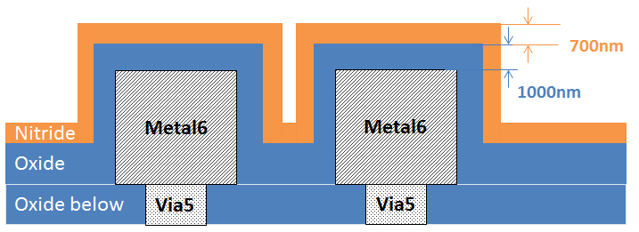
In most EM simulations of on-chip layouts, the passivation is assumed planar, so that we can easily simulate it with Sonnet or Momentum. However, in real life the top metal is often coated with a conformal passivation.
This does not mean that planar EM simulation is invalid. Most planar simulations agree well with measurements, because the influence from the “3D” passivation is small for large conductor width. For narrow conductors, narrow spacings or other sensitive cases, we can do a quick worst case test, and vary the planar dielectric properties between the extremes (smallest possible value is air erel=1, largest value is erel ~8).
But how about doing a more accurate test with the Full-3D FEM solver built into ADS? That’s what this application note is about: configure ADS to automatically build the correct, full 3D passivation for FEM simulation.
This application note is partially based on prior work from Agilent AE Ludwig Eichinger. Many thanks, Ludwig!
The Idea – 3D Passivation
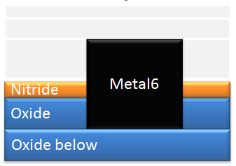
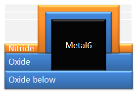
By combining a planar substrate with dielectric vias, we can represent the 3D passivation. This section gives you an overview of the method, before we go into the implementation details. We start from the conductor metal …
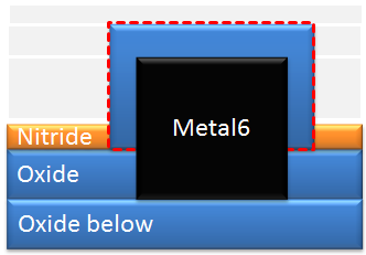
… and the add a dielectric via to represent the oxide.
In the overlapping area between oxide and nitride, the oxide block wins and pushes away the planar nitride.
In the overlapping area between oxide and metal, the metal wins.
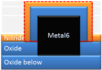
Then, we add another dielectric via for the nitride.
In the overlapping area between oxide and nitride, the oxide block wins and pushes away the nitride block.
In the overlapping area between oxide, nitride and metal, the metal always wins.
As you can see, we have multiple overlapping materials, and the key is to assign the correct priorities (“precedence”). Using priorities, we can avoid boolean operations on overlapping 3D objects. We will address priorities below, when the dielectric vias are defined.
Derived Layers
To build the passivation geometries from the Metal6 geometries, we will use the “derived layer” concept that was introduced in ADS2011. Another application of derived layers had been discussed in the application note on via merging.
In total, we need three derived layers for the FEM passivation: one clone of the top metal layer, and two dielectric vias for Oxide and Nitride. This will explained in detail below.
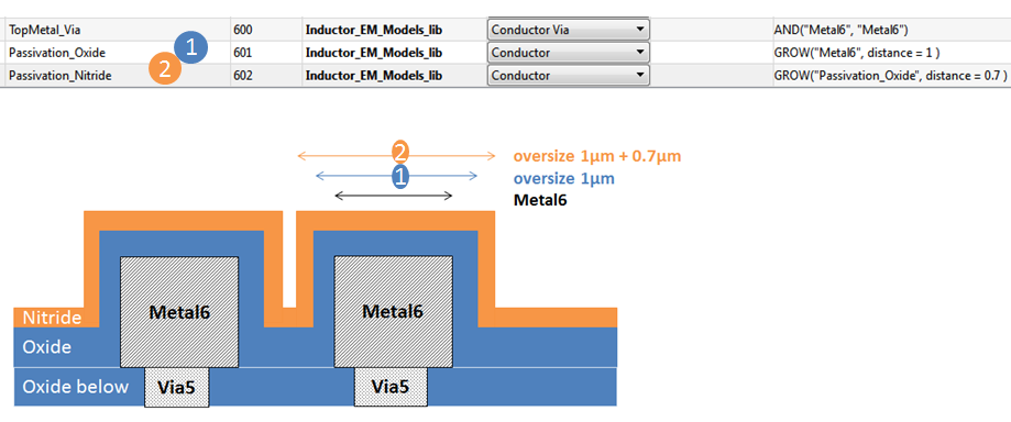
Layer “TopMetal_Via” is created as a clone of Metal6. This is required for a workaround where we need thick metal that penetrates through multiple dielectric layers. The clone is created by boolean AND of Metal6 with itself.
Layer “Passivation_Oxide” is created by horizontally enlarging the metal6 outline by 1µm on each side. That is the additional thickness of the oxide on the conductor sides. Layer “Passivation_Nitride” is then created with an additional 0.7µm.
Note that this is only the horizontal increase in size. Next, we will deal with the dielectric stackup.
Defining the dieelectric stackup
Automating the 3D passivation for FEM requires a combination of
- derived layers that we can map to dielectric vias,
- precendence rules to define which material “wins” in overlapping areas and
- a trick to create thick Metal6 that passes through multiple dielectrics.
First, we need to set up the (infinite) dielectric layers. This determines the stackup far away from metal6, and it determines possible locations for dielectric vias (for the passivation).
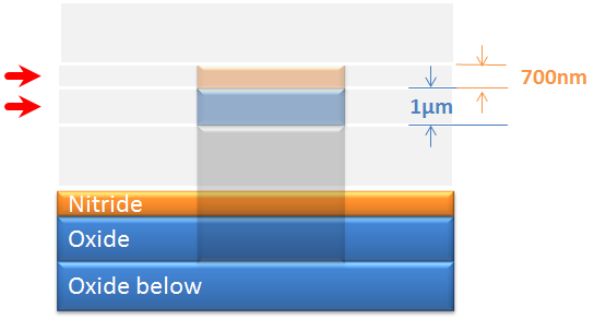
We start with an “empty” substrate: In places where we have no Metal6, the passivation starts at the same level where the bottom of metal6 is (indicated with the hatched line in the picture below). We have 1µm oxide and 0.7µm nitride.
The next layer is air, and it ends at the top of Metal6. The thickness can be calculated from the Metal6 thickness (3µm) and the passivation thickness (1µm + 0.7µm). Then, Metal6 will pass through the oxide layer (1µm) and the nitride layer (0.7µm) and penetrate another 1.3µm into the air above. We need an air layer above the nitride with a thickness of 3µm – 1µm – 0.7µm = 1.3µm.
Next, we will apply the oxide above Metal6. For this, we need an additional air layer with 1µm thickness, located above Metal6. This air layer can be used to locally insert the “oxide” dielectric. Next, we will apply the nitride on top of the oxide. For this, we need an additional air layer with 0.7µm thickness. This can be used to locally insert the dielectric via for nitride.
Above that air/passivation layer, we have air with open boundrary.
Top Metal Conductor
Now that we have the basic stackup with proper layer thickness, we can define the Metal6 conductor.
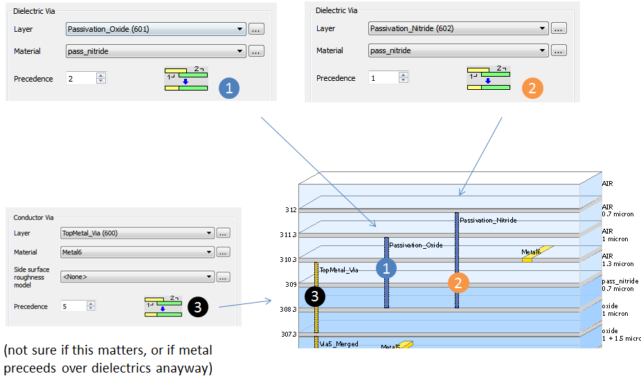
For this, we need a workaround: In the 3D stackup, the metal will pass through multiple dielectrics. The FEM solver can simulate this thick metal, but the substrate editor does not allow it for “normal” conductors. The workaround is to define the metal as a conductor via, which passes through multiple dielectrics.
And again, we need a workaround: the Metal6 geometry is included in the substrate as a via now. ADS allows you to attach pins/ports to metal conductors, but not to vias. However, it does support another layer that has only the pins/ports. We need another layer because ADS substrates do not allow to map the same layer twice. So here is the second workaround: In the derived layers, we had created a “clone” copy of Metal6. Now, we can map the original Metal6 layer for the pins and map the cloned layer for the 3D metal (the via which represents the Metal6 conductor).
Note the checkbox “Only pins and pin shapes from this layer”. This tells ADS that the via is the only conductor for Metal6, and we only use the pins from the other copy.
Dielectric Vias
Now, we can finalize the substrate by adding the dielectric vias for the passivation.
What is important here is to properly prioritize the materials:
- Nitride has lowest priority.
- Oxide wins if it overlaps with nitride.
- Metal6 has highest priority, and wins if there is any overlap with other materials.
In ADS, priority for overlapping materials is set with the “Precedence” value. Larger number means higher priority.
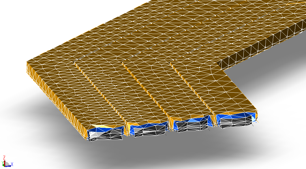
Note that precedence is evaluated by the solver, and not visible in the 3D viewer. In the EM preview, Metal6 and the dielectric vias for passivation will be shown as overlapping objects. This doesn’t cause any problems, because the solver knows what to you. To check that, and really see the resulting 3D objects, we will look at the 3D mesh later.
Example
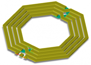
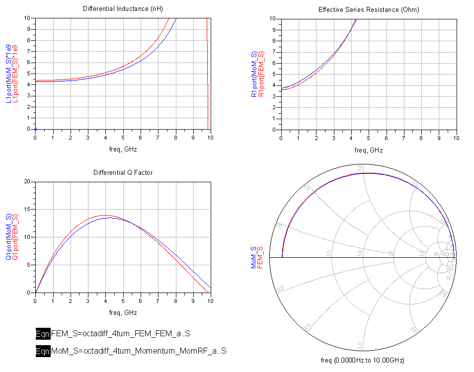
Let’s apply this FEM simulation with 3D passivation simulation to an example inductor, and compare results to Momentum. The inductor in this example has conductor width w=10µm, conductor spacing s=4µm, N=4 turns and an outer diameter of 250µm.
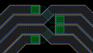
Usually, derived layers are not shown in layout, but we can force them to be shown. This is what we see in layout if we force the derived layers to be displayed: dark gray is the Metal6 outline, blue is the +1µm oversized oxide and orange is the 1µm + 0.7µm oversize nitride.
As mentioned before, the 3D EM preview does not evaluate the priority of the overlapping materials. To see the final passivation “shell” around the metal, we need to look at the FEM mesh after simulation. Simulation was done with volume meshing for the conductor (“meshed interior”).
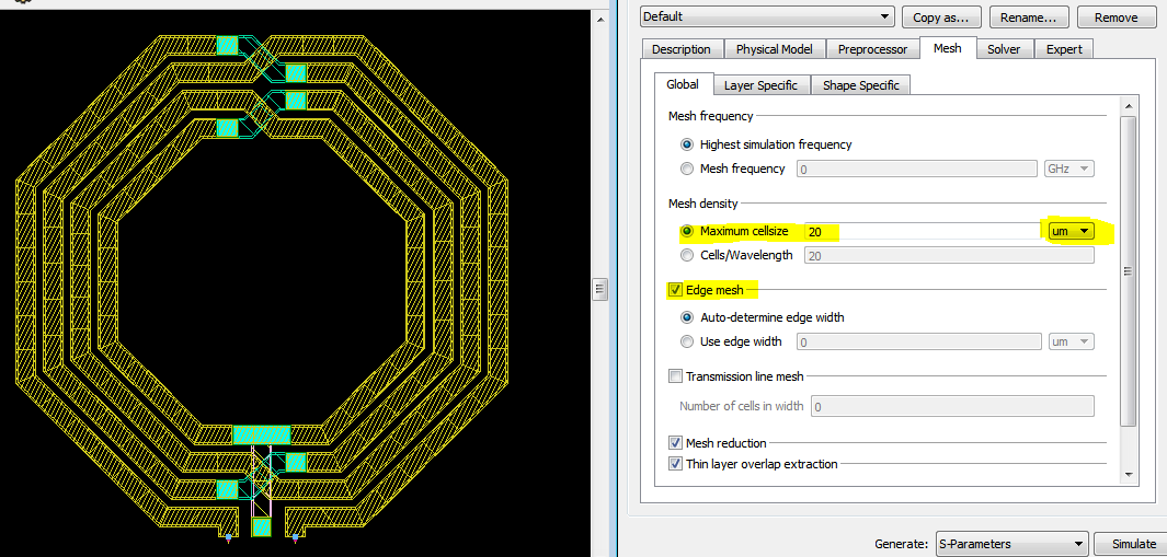
For comparison, another simulation was done with Momentum RF mode, using the simple planar substrate. Mesh settings have been tweaked for good accuracy, with a maximum cell size of 20µm.
For this example, Momentum results with simplified planar substrate and results from FEM with full 3D passivation are quite similar. This confirms that the planar substrate in Momentum is appropriate in “normal” cases, where the dominant capacitance is from the bottom side of the conductors, and the influence of the side wall capacitance between adjacent traces is rather small. For narrow conductors, the relative effect of the side walls is larger, and a stronger effect is expected.
This ends our application note on ADS EM models with full 3D Passivation for FEM simulation.
To receive the example project, please send an email to support@muehlhaus.com

