
Controlled Impedance Line Designer is a great tool for designing transmission lines in RFIC technology. Initially, this tool was part of high speed digital license bundles, but it is now available to all ADS users (requires ADS core license).

Controlled Impedance Line Designer (CILD) provides two very useful features:
- Line impedance calculation and line synthesis for complicated stackups, based on a Momentum substrate file
- Transmission line models for use in schematic simulation can be created easily
There is no need for using pre-calculated data tables, and no need to create schematic model stackup definitions manually. Models will be created “on the fly” from the line type and corresponding Momentum stackup. This is great for complicated RFIC stackups, because it is so efficient and easy to use!
Requirements on the Momentum stackup file
There is one requirement for using CILD: the substrate file must not include semiconductors. Ooops !?
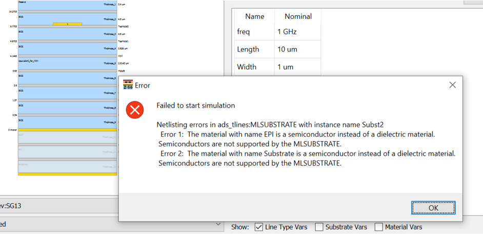
What sounds like a show-stopper is not a practical problem because we want to create microstrip lines which have a metal ground plane, and that ground plane shields the line from the silicon substrate. Which means that it doesn’t matter what material we have below the ground shield. We can simply create a copy of the Momentum stackup where we replace silicon by a normal dielectric with epsr=11.9
The steps to create the modified substrate copy are simple:
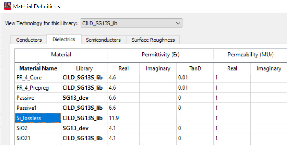
- Copy the Momentum stackup from the PDK to your workspace library
- Create a new dielectric in your workspace libary using Options > Technology > Material Definitions , with er=11.9
- Give that new dielectric a meaningful name (e.g. Si_lossless) and replace the Silicon layer(s) in your stackup copy with that new dielectric
That’s all, the new stackup with dielectric instead of semiconductor can be be used with CILD. The material is below the ground layer, so the modification has no effect on line properties.
Using CILD to analyze and synthesize line dimensions
To start CILD, open the stackup in Momentum substrate editor and click on Tools > Controlled Impedance Line Designer.
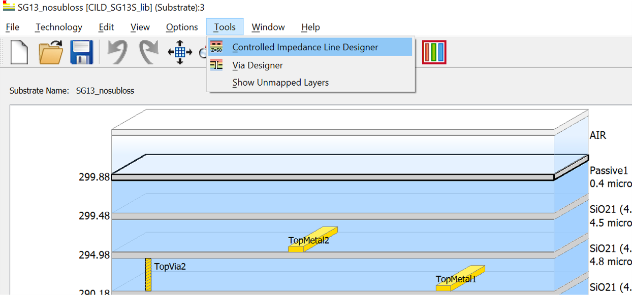
This brings up the CILD window as shown below: We can choose line type, layer combination and line geometry parameters. In this first example, we design a single microstrip on TopMetal2 over Metal1 ground plane. Top plane is set to None because we have an open boundary on top (no metal shield on top).
By clicking on the gear icon, analysis starts and we find 79.9 Ohm line impedance for the 5µm line width given here. In addition, we find information like attenuation and effective dielectric constant.
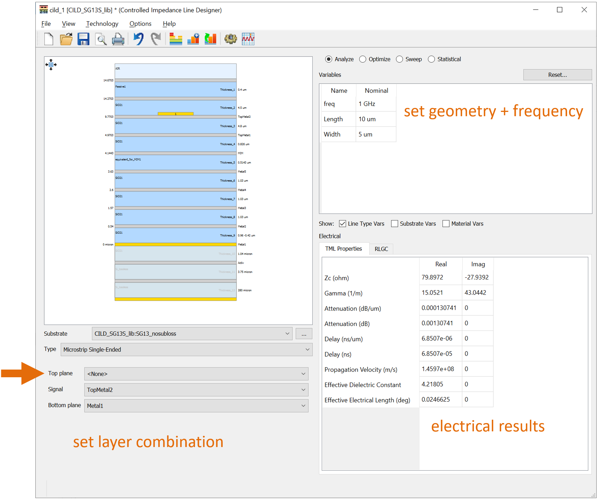
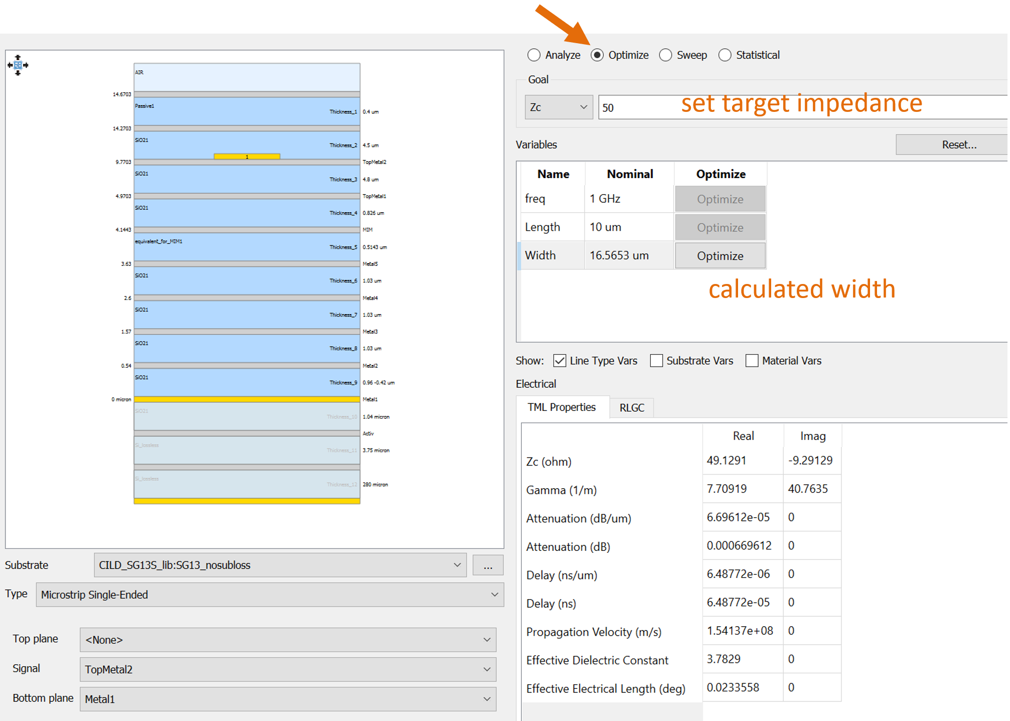
To find the required width for a target impedance, we can switch to Optimize and let CILD calculate the value by pressing the “Optimize” button next to the Width field. Note that line impedance for RFIC lines will increase at low frequency due to line resistance, so please specify the actual RF frequency!
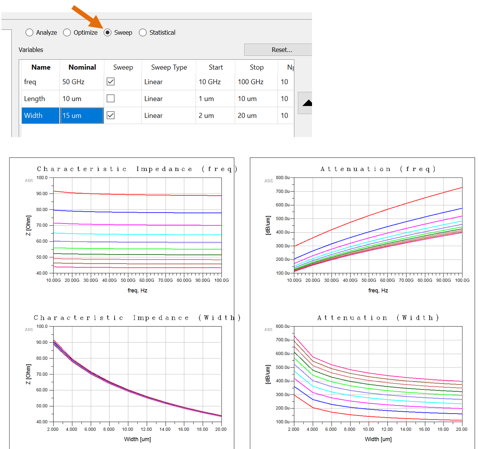
Another option is the “Sweep” function that allows to sweep multiple geometry parameters and create nice design tables.
These analysis and synthesis features (similar to good old Linecalc for simple stackup) are only one aspect of using CILD. The second aspect is even more interesting: we can now create a line model for use in schematics, so that we can quickly design line structures for these complex stackups!
Creating a Line Type for use in schematic simulation
To simulate transmission lines in schematic, we can create a “Line Type Definition” from Controlled Impedance Line Designer. This will convert the Momentum stackup into a format that is understood by the line model, we only need to define the corresponding line geometry (e.g. single microstrip) and define the signal and ground layers. For each layer combination that we want to simulate, we need a separate Line Type Definition.
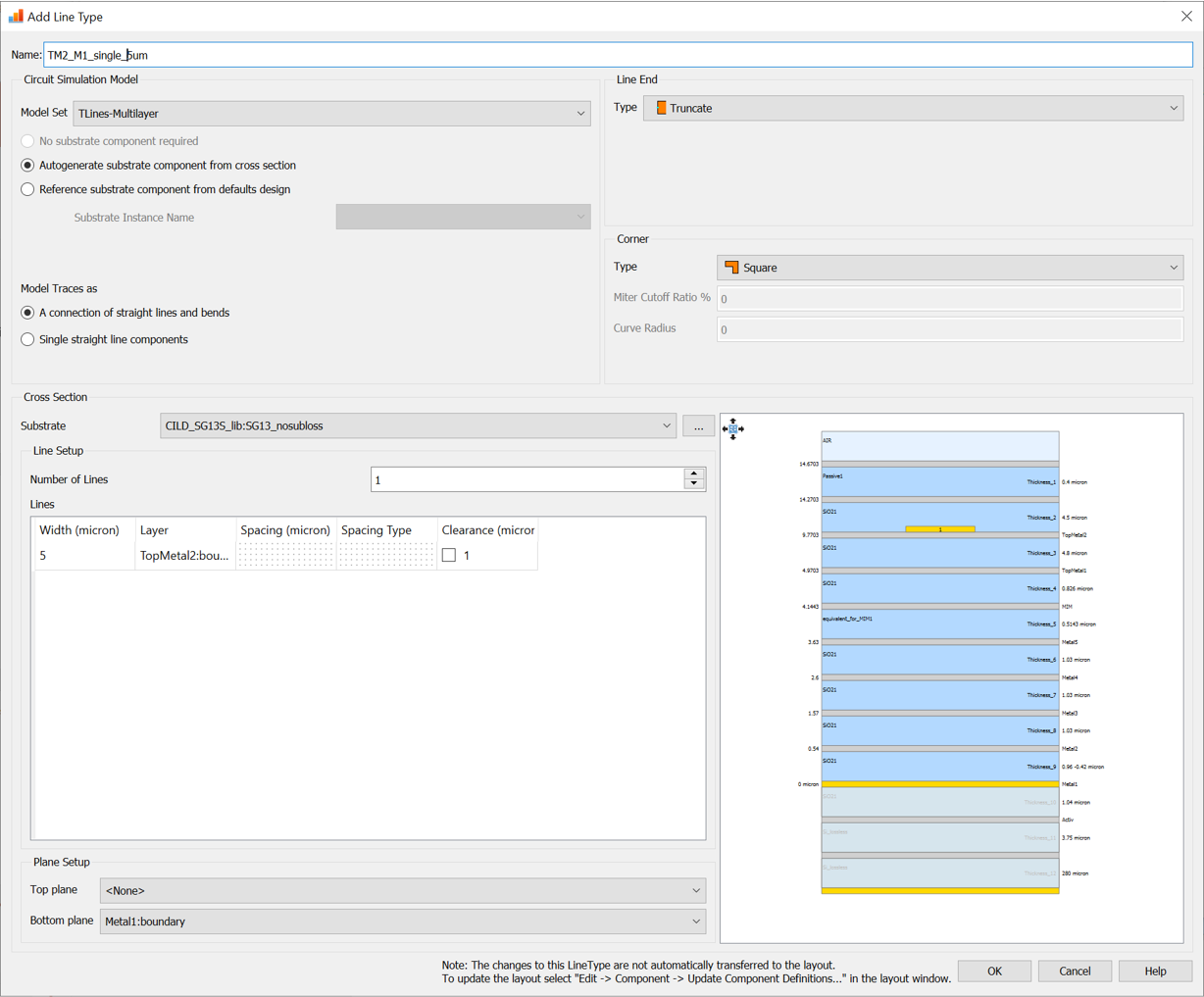
To create a new Line Type Definition from CILD, use menu item Technology > Add New Line Type Definition To Library…
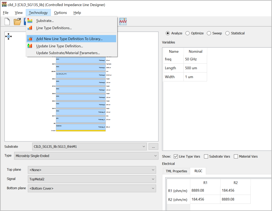
This will bring up a dialog where you can define layer geometry including default width, as well as layout routing options for this line type. We leave the Model Set option as “TLines-Multilayer” and use “Autogenerate substrate component from cross section”. For the model name, we use a meaningful name that describes the layer combination used in this stackup. When clicking OK, the new Line Type Definition is stored to the library.
In schematic, the new Line Type Definition can be used with line models from palette “TLines – Line Type”. Line model parameters are line length and line width, the stackup is described by the line type. Specifying the width is optional, you can also use the default width defined in the Line Type Definition.
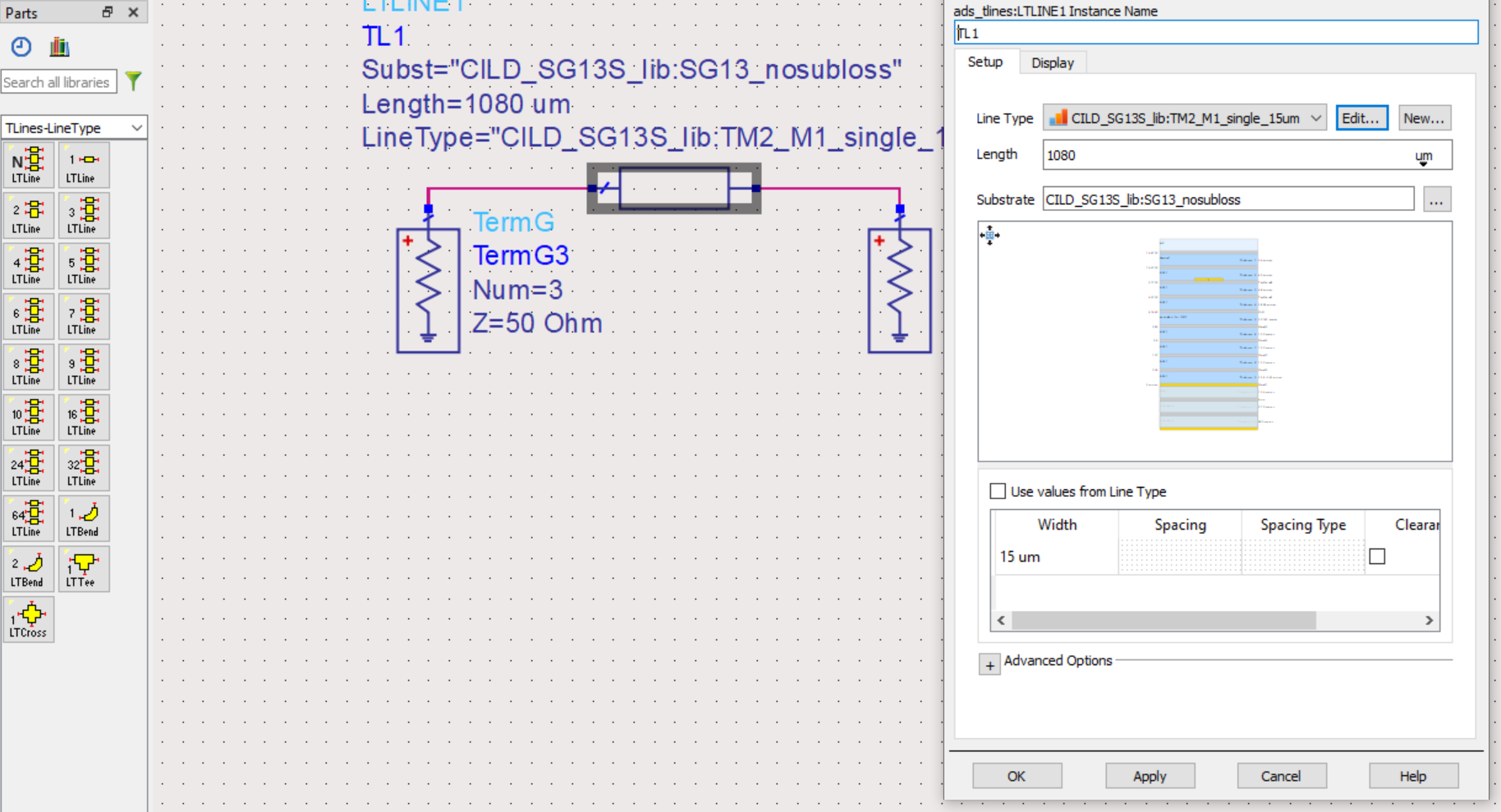
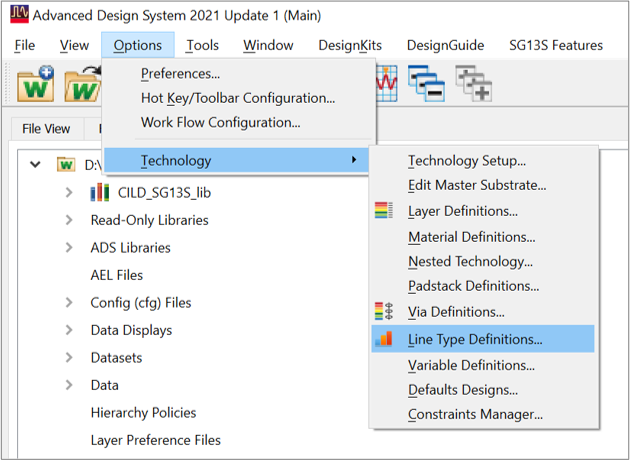
If you want to see/edit/modify an existing Line Type: these can be found in the library technology dialog from ADS main window, menu item “Options > Technology > Line Type Definitions…
Using Line Type models: notch filter example
To show the use of LineType models, we use a little example with two open ended lines forming a notch filter. Layer combination is TopMetal2 over Metal. In this example, all lines are 15µm wide, but it would be easy to use other mixed line widths.
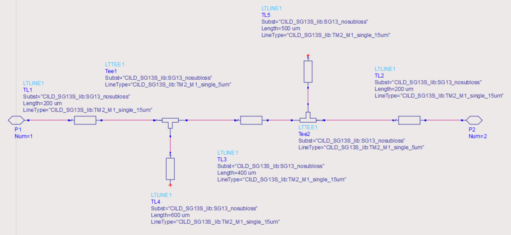
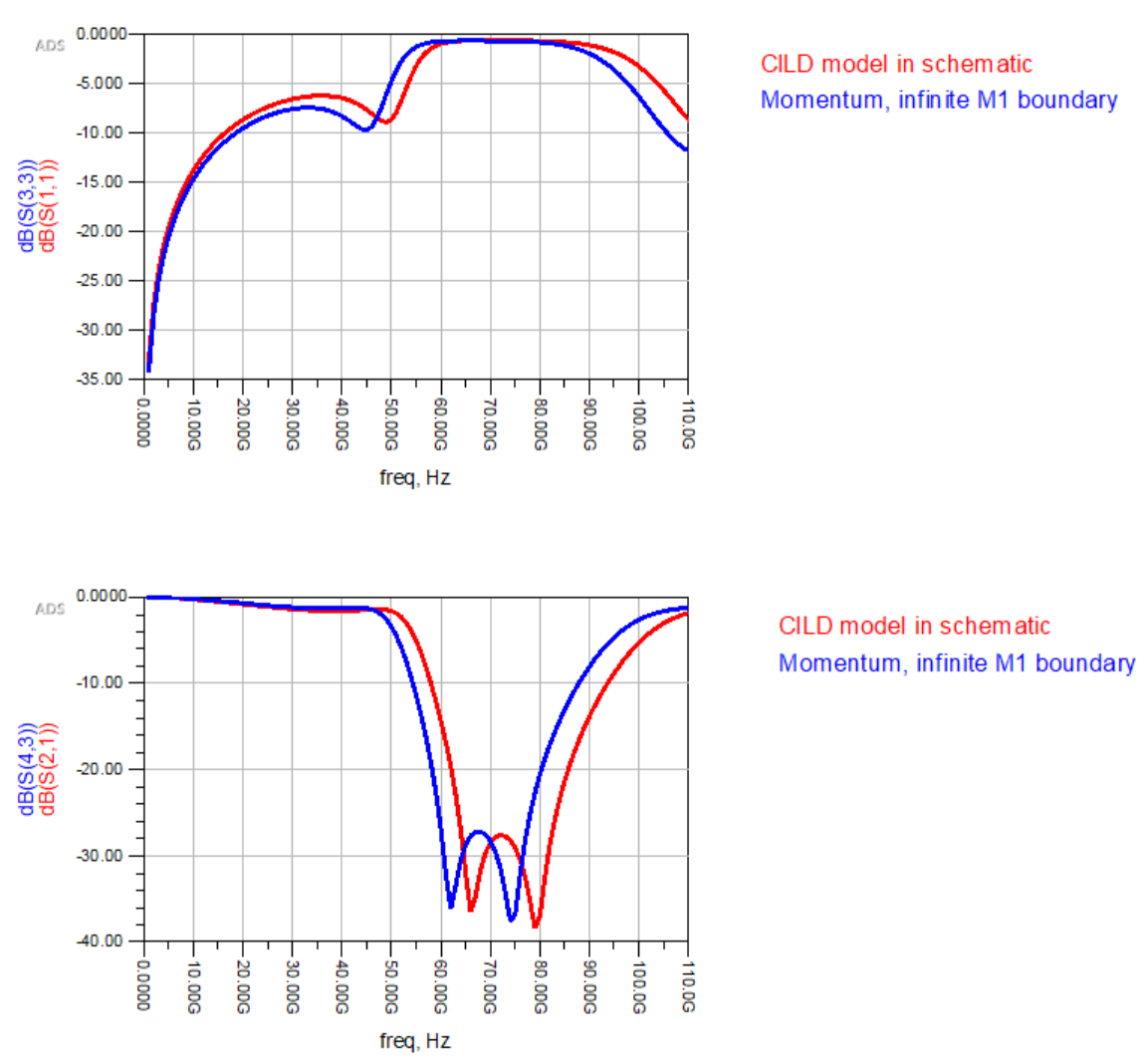
For comparison of models and full EM, the layout for this circuit was auto-generated and Momentum EM simulation was run to get the response of the full structure. This includes all couplings between all elements, whereas the schematic models only connect through the circuit nodes (no field coupling between elements).

Agreement of results is quite good, with only a small shift in resonances. Schematic models are very useful here to quickly design an initial version, which can then be verified by full EM simulation.
Other line types and discontinuities
CILD and LineType models are not limited to simple microstrip lines. They also provide models for multiple coupled lines as well as BEND, TEE and CROSS discontinuities.
Summary
ADS Controlled Impedance Line Designer was initially designed for high speed digital PCB, but it is a very useful tool for RFIC stackups also. Key features are line impedance analysis, line synthesis and line model for use in schematic simulation. The latest ADS releases include CILD with the ADS core license, so it is available at no extra cost.
Supported line types include single lines as well as coupled line, with or without side ground. For use on silicon substrates as shown here, one simple modification to the Momentum stackup is required. Models with that modified substrate are valid as long as a bottom ground shields the line from the silicon substrate.