
This is part 2 of the design report on a 432 MHz high pass with 144 MHz rejection. Part 1 can be found here.
When I published the initial design, readers asked about the effect of the box on filter performance. Indeed, the filter was initially designed by simulating the PCB only, without including the box during design/simulation.
Based on reader questions, I had added measurement and simulation of the boxed filter in part 1, and some small frequency shift was observed indeed. We will now study that effect in more detail, and further optimize the filter performance.
Baseline design – measured and simulated
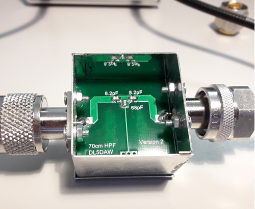
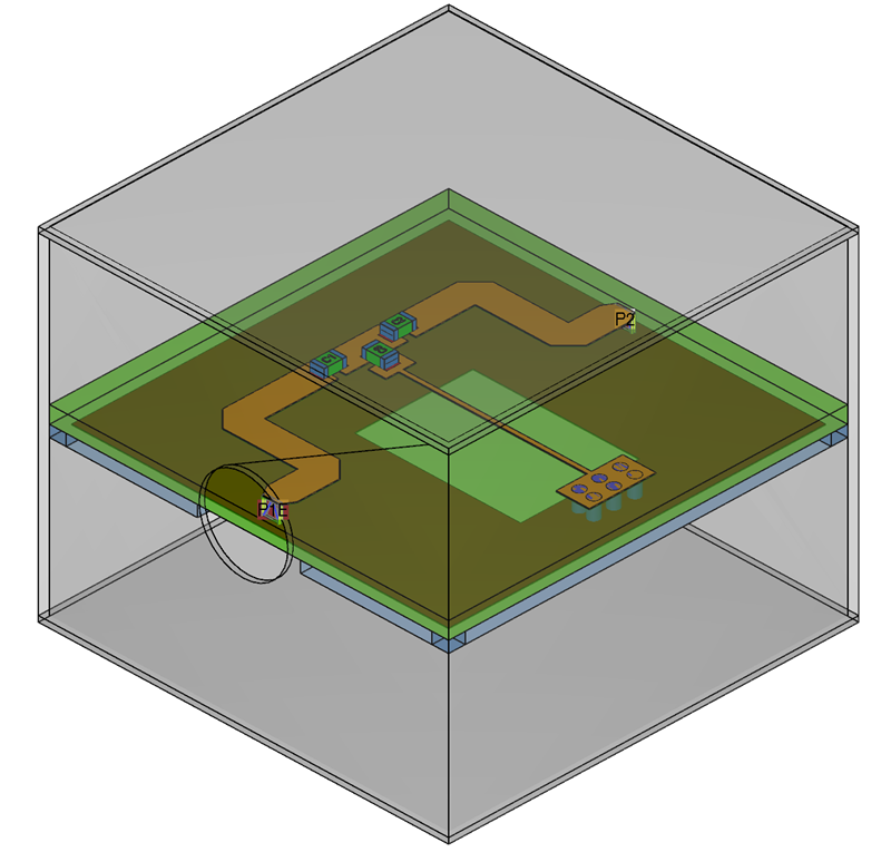
As a baseline simulation, we place the 34mm x 34mm “no box” design inside the metal box. Empire XPU is used for simulation, with 3D SMD models in 0805 size, 8.2pF for series and 68pF shunt.
Measured and simulated results for that PCB are compared below. Both S11 and S21 show excellent agreement, so we can use EM simulation to optimize the filter response.
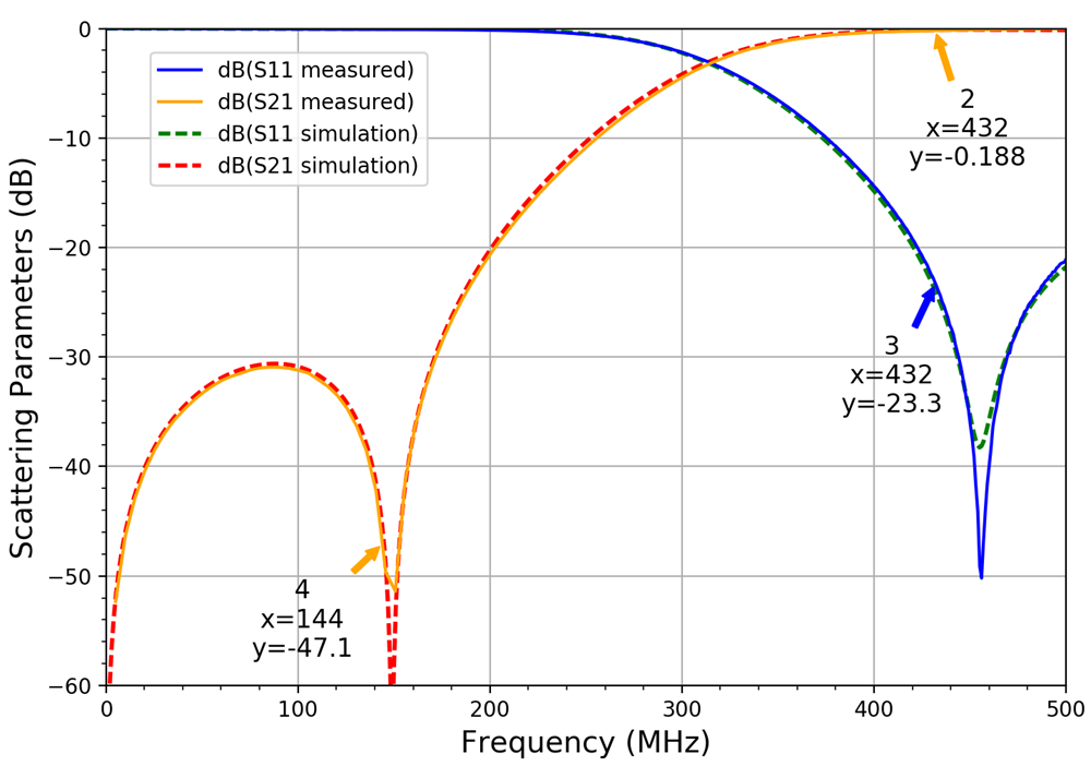
Stop band rejection is 47dB already, and insertion loss at 432 MHz is less than 0.2dB. But there is still some room for improvement: both stop-band notch and pass band matching are shifted up in frequency a bit. Let’s fine tune that!
Ground cutout underneath the inductor
The cutout in ground was already designed using EM simulation, to reduce the length of the “shunt inductor” line, but didn’t account for the box ground. Now, cutout dimensions will be tweaked to fine tune the response.
Current density at 144 MHz is shown below, showing very clearly where return current flows around the cutout. So that is our approach to tune inductance: tweak the cutout size!

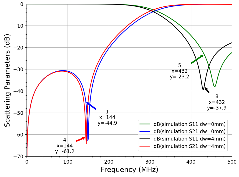
Tweak it! Parameter sweep for cutout width
A parameter sweep is defined with variable dw that adds 0 to 4 mm additional cutout width.
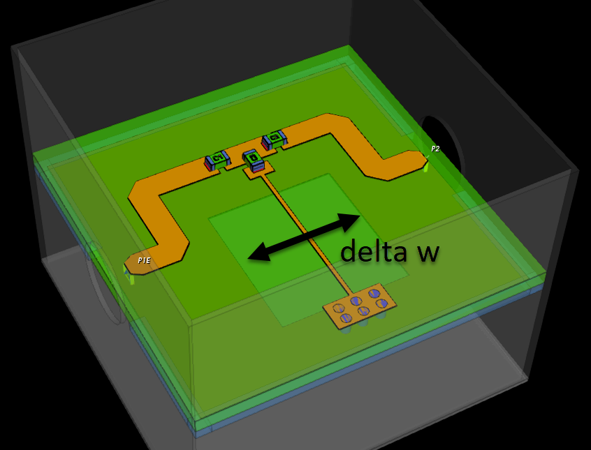
Increasing the cutout width moves stopband notch and passband S11 minimum down in frequency, as desired.
With +4mm extra cutout width (2mm on each side), we can place the stop band notch at 144 MHz and at the same time have minimum reflection at our 432 MHz target. That means we are precisely back on target, as initially designed for the unboxed PCB.
Knives out – Check the tuned performance in measurement
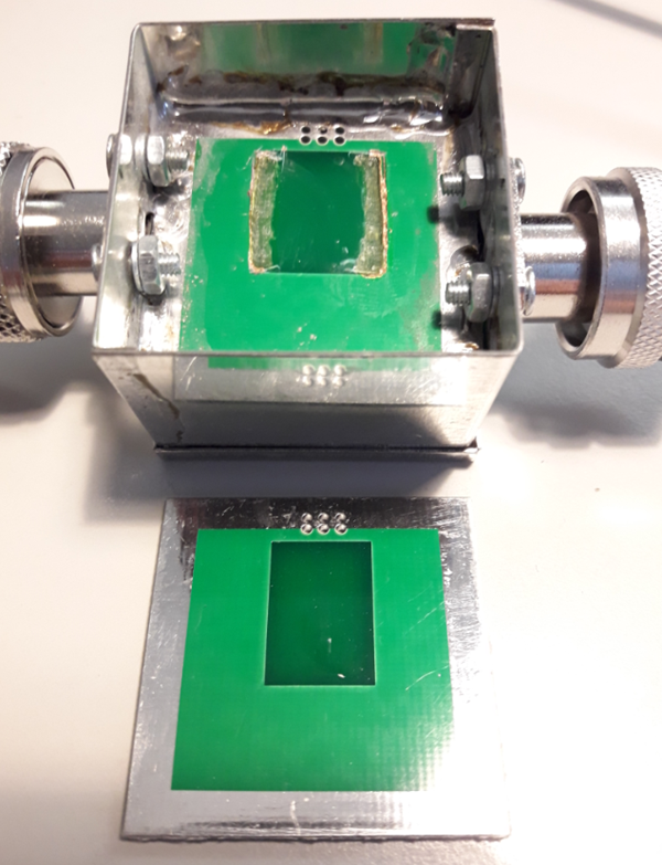
Based on the previous excellent agreement between measured and simulated, we can be quite sure that this modified layout will work. But reality check is always useful, so I tried to tweak the hardware and increase the cutout by 4mm total, i.e. 2mm on each side. This manual cut doesn’t look very nice, but works as a reality check. For comparison, the photo shows another PCB with original dimensions.
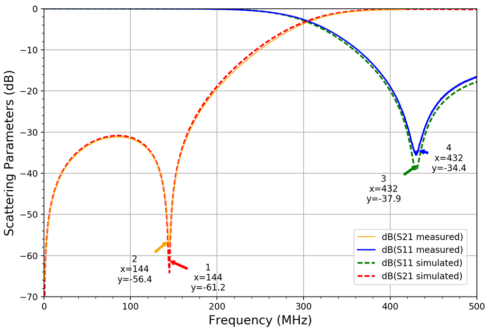
Measurement confirms the tweak found in simulation: frequencies shift down, very close to the target values.
Stop band rejection is 56 dB now, instead of 47dB.
Return loss is optimized for 432 MHz and better than 30dB now, instead of 23dB using the original layout.
Lessons Learned and Summary
I should have done this simulation before sending the PCB for manufacturing! Thank you for comments asking about the box influnce – it does matter when looking for perfection. Ground path inductance is just as important as signal path inductance, and we do have some small signal/ground path change here.
Version 3 layout in Gerber format, with the increased cutout width: hpf432_artwork_34mm_V3.zip
Empire XPU 3D EM model including the box: hpf432_boxed_V2_sweepcutout.zip
More information on EM simulation with Empire XPU EM
More information on our consulting services