[two-thirds]
A new release of the m/matl EM Technology File Editor is now available.
New features:
- Import of technology information from Cadence Assura procfiles
- Export to Empire XCcell 3D EM
- Export to Asitic tek file (beta)
For more information and download, click here.
Import from Cadence Assura procfiles
You can import substrate information from existing Cadence Assura procfiles.
To use this option, use File > Import and select an Assura procfile. The software will evaluate the procfile, and also try to find and evaluate two additional files in the same directory: p2lvsfile and lvsfile. If these additional files are not available, the via information is missing and you need to set the via layout (from… to …) manually.
Unfortunatly, the layer names used in the Assura files do not always agree with the layer names used in the layout editor. During import, m/matl tries to figure out the layer names, as best as it can. Sometimes, this is not possible and you need to set the correct Cadence layer names manually.
Important limitations for using Assura procfile import:
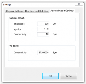
It is important to understand that the substrate itself is not included in any of these files. The substrate thickness, permittivity and conductivity are added based on m/matl default values. These default values can be set with File > Preference > Assura Import Settings.
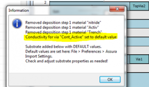
In this dialog, there is also a settings for via conductivity. The via conductivity might be defined in the Assura files, or it might be missing. If the information is missing, the default will be used and this default assigment is listed in the import summary message.
Another note in the import summary message is related to the deposition steps. At the surface of the substrate, there are multiple deposition steps 1 defined, for different areas of the chip. The m/matl import uses only the first line for deposition step 1, which is usually for field oxide, and skips the other deposition step 1 entries. These skipped lines are listed in the import summary message.
For metal sheet resistance specified in the p2lvsfile as (Ri,wi) pairs for width dependent sheet resistance, m/matl uses the last entry, which is supposed to be valid for widest metal traces.[1]
Carefully check your results! The Assura import has been tested and optimized with many different design kits. However, there is some “educated guess” required in some cases, especially for layer names. If you experience problems, please let us know!
[/two-thirds]
[third] [/third]
[1] From the Assura documentation: “Additionally, the (ri,wi) pairs should be specified in order of increasing width.”


