
This application report describes a PCB high pass filter for the 70cm band (432 MHz) with approximately 50dB rejection in the 2m band (144 MHz), which requires no air coils and no trimmer capacitors. Simulations and measurements are shown.
The filter is designed for multi-operator HAM radio contest stations working on both bands simultaneously, on the same site. It is placed in the receive path in front of the 432 MHz low noise preamp, to avoid overloading the LNA with strong signals from the 144 MHz station.
The filter was designed from a practical requirement – in our contest location, we did have enough low pass filtering to avoid trouble from the 3rd harmonic of the 144 MHz signal, but the 144 MHz fundamental (!) picked up by the 70 cm antenna was driving the 432 MHz LNA into nonlinearity. That’s why we decided to add an additional high pass filter in the 432 MHz receive path, which indeed solved that problem.
Starting point: VE2ZAZ design
Initially, we used a design created by Bertrand Zauhar, VE2ZAZ, as described here:
http://ve2zaz.net/HighPass_Notch_Filter/432HighPass144Notch.htm
That design is quite large and uses two wirewound shunt inductors and three tunable capacitors.
In simulation, using ideal components, that design provides rejection of around 60dB at 144 MHz and almost perfect transmission at 432 MHz. And indeed, Bertrand describes his measurements like that, with 60dB rejection and around 0.1dB insertion loss. See the link above for Bertrands setup and measurements.
The VE2ZAZ design works great once tuned properly. However, our filters based on this design required very careful tuning of the handmade wirewound inductos and the trimmer caps to achieve that performance. Component values are a challenge to reproduce.
New design with no trimmers and no air coils
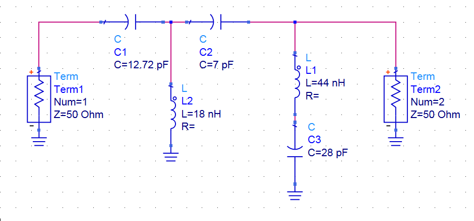
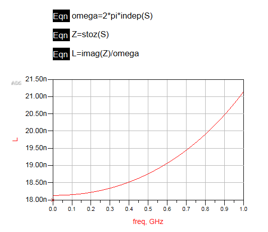
Our idea was to create a modified design that requires no air coils and no adjustment/trimmers, based on careful and detailed simulations upfront. Simulations using Keysight ADS circuit simulation showed that this should be possible with a slightly simpler T configuration, with shunt path LC of 68pF and ~18nH to notch out 144 MHz.
The shunt inductor was designed as a 0.5mm wide line on standard 1.5mm FR4, with a ground cutout below. The cutout helps to increase inductance, and cutout size was tweaked to achive the ~18nH inductance calculated from circuit simulation.
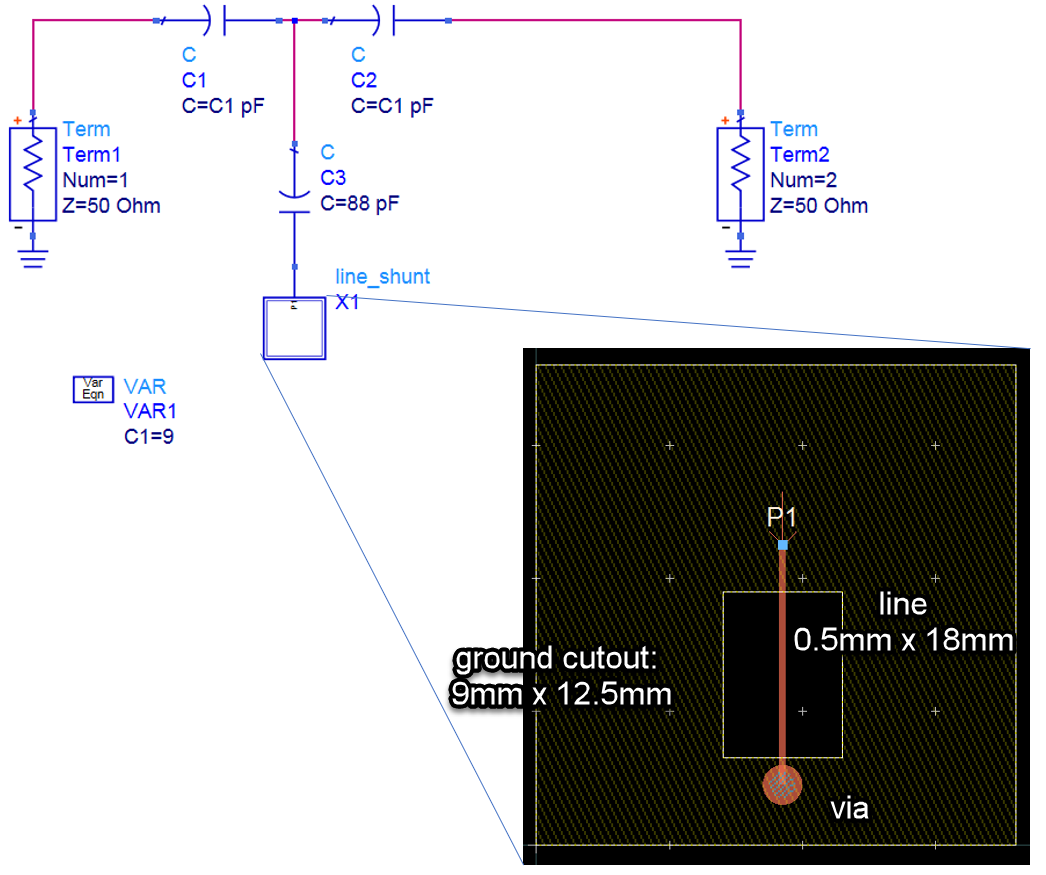
EM simulation using ADS Momentum was performed to simulate that part of the layout, calculate the corresponding series inductance and tune it to the desired ~18 nH.
The full layout was then created, with a PCB size of 37mm x 37mm. The schematic below shows the co-simulation setup for the complete filter.
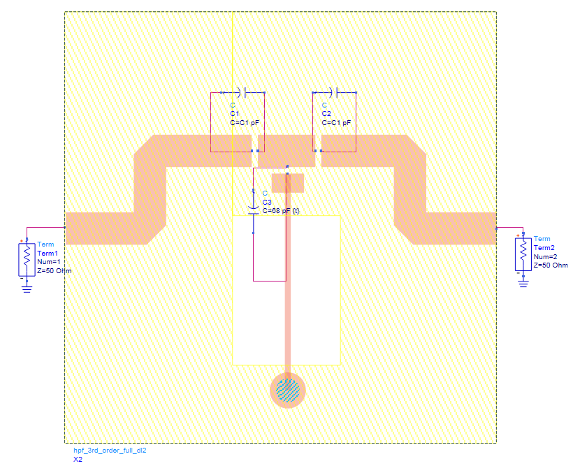
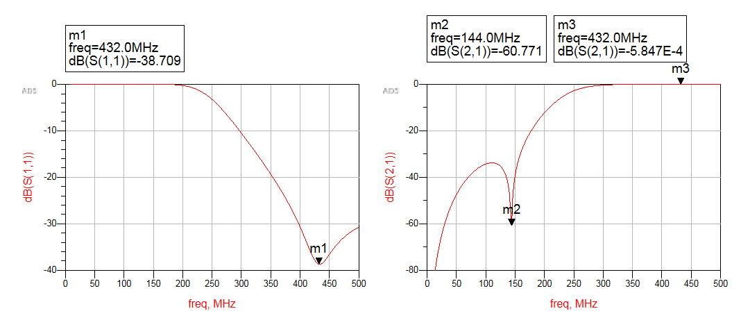
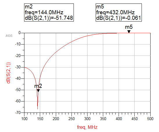
For that design, co-simulation of layout and SMD promises 50 dB rejection at 144 MHz and insertion loss <0.1 dB at 432 MHz.
This reaches our design goals, so the design idea looks feasible and we can move on and create the final layout.
Final layout and measurement results
As a last minute change, the single large via from simulation was replaced by an array of smaller vias. Simulation was not repeated in ADS for that final layout, because changes are expected to be small, and we expected some tuning of capacitor values in the final hardware anyway.
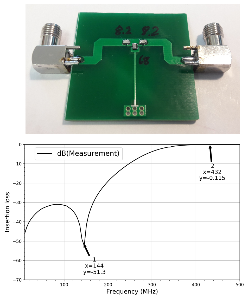
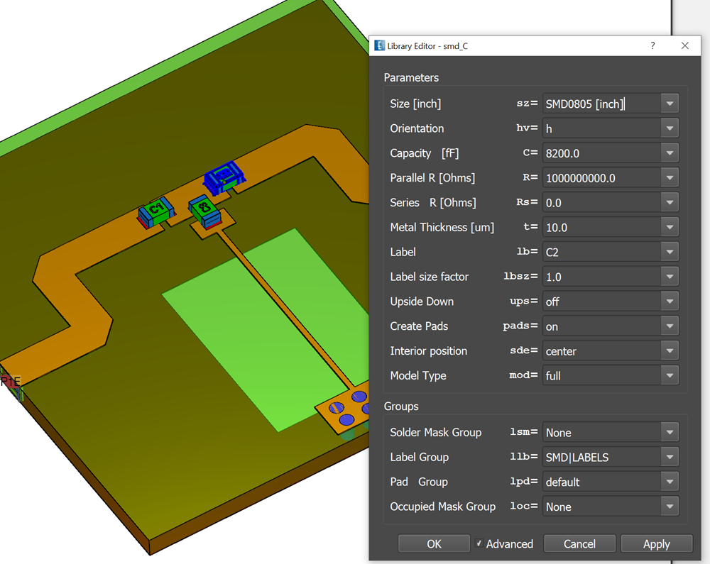
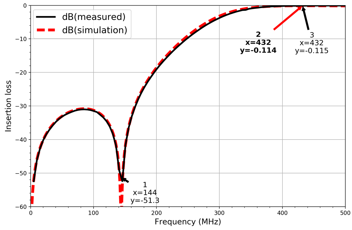
Measurements were performed in the home lab using a simple low cost VNWA3 network analyzer. For series capacitors, 8.2 pF in 0805 size was used instead of ideal 9 pF from circuit simulation. The shunt capacitor was 68pF in simulation and measurement, no change required.
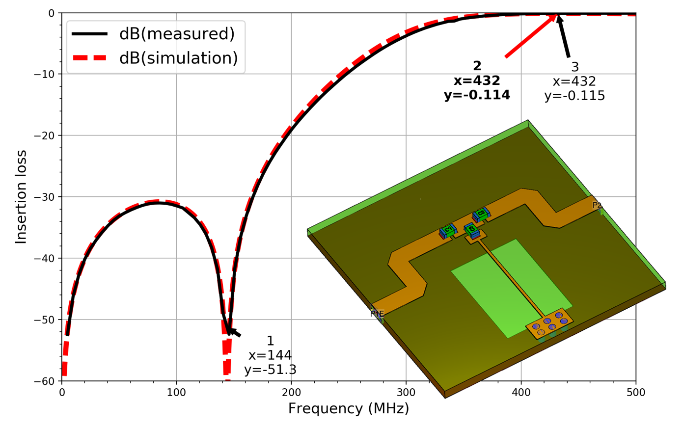
Indeed, the filter performs nicely out of the box, with approximately 50dB rejection at 144 MHz and ~0.1 dB insertion loss at 432 MHz.
At higher frequencies, the dynamic range of the VNWA3 analyzer used here is limited. It is a low cost device and switches to using harmonics of the internal source above 500MHz. Also, VNA calibration accuracy is limited, providing only ~20dB of receive port matching at high frequency for our test case. For that reason, measurement results above 500 MHz are less accurate.
Full 3D EM simulation with SMD
Just for fun, we also created a 3D EM model of PCB + SMD in Empire XPU and compared that to measurement results. SMD components with 8.2pF and 68pF are included as full 3D device models.
Good agreement is seen between measurement and 3D EM simulation in Empire XPU.
What happens if we place it in box?
Above, the filter was simulated and measured without a surrounding box. Some readers wondered how much the “inductor” line over cutout is affected if we place the PCB inside a metal box, which provides additional ground paths.
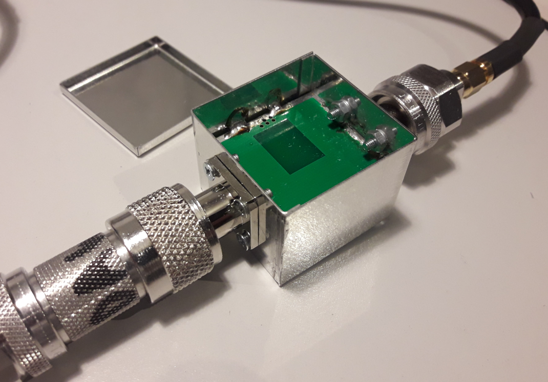
For practical use, that box is required indeed. When designing the filter, I wanted to place it inside a standard 37mm x 37mm box, but didn’t realize that those 37 mm are the outer box dimensions, and created a PCB that is slightly too large. So I had to cut the edges of the PCB to squeeze it into the box. An updated version of the layout can be found for layout at the end of this page.
I assembled a second PCB, with the same nominal values, and squeezed it into the box as shown below. The distance from the PCB ground to the bottom cover of the box is approximately 10mm.
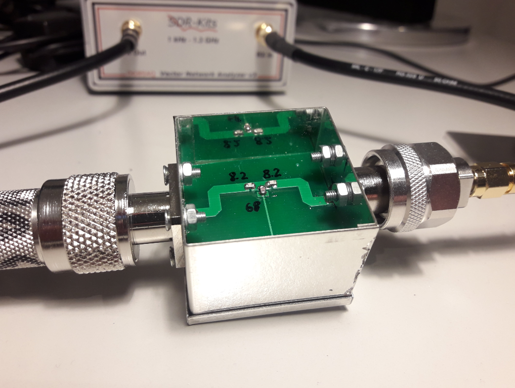
PCB ground is soldered to the box at the connectors and in some additional places.
With this PCB in a box, the 144 MHz notch is shifted by +5 MHz compared to the other unboxed PCB. That result is very stable and does not change when the top and/or bottom covers are removed.
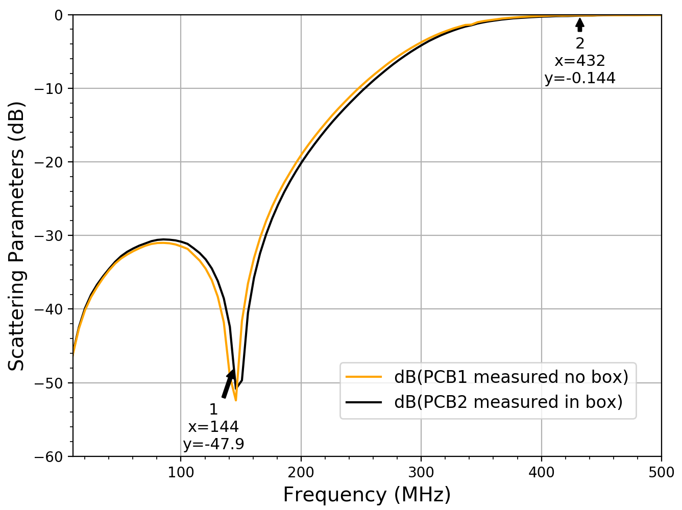
It wasn’t clear if the shift in frequency is caused by the box itself, or by component/assembly tolerances. So here is another simulation to check that:
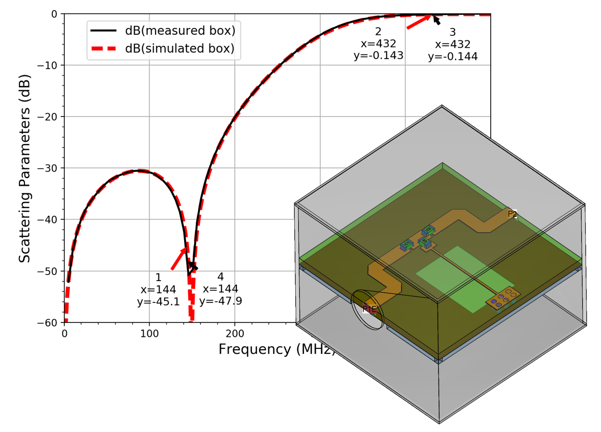
Indeed, the box (return path through side grounds?) does cause that small shift in frequency. We see that effect in both simulation and measurement!
Power handling
When presenting the filter to HAM radio friends, they stared at the small 0805 SMD capacitors and wondered what the power handling the filter might be. Good question indeed – it is designed for receive path only, which sounds safe, but what voltages at the SMDs are expected then if we have a 750W station at 144 MHz operating close to the 432 MHz antenna with LNA?
To find out, we do an AC simulation with a power of 1 W (30 dBm) crosstalk into the 70cm receive path.

With that testbench, we get the results show below: the maximum voltage for 144 MHz input is 18.7 V (peak) at C1. The peak current in the shunt line is 153mA then. Both values are safe.

Downloads
The inital PCB was designed for 37mm x 37mm PCB size, and simulations and measurements above all refer to that size. The Empire XPU simulation model for the 37mm x 37mm layout can be downloaded here in Empire 8 *.emx format: hpf432_verticalport
It turned out that it’s better to shrink the PCB to 34mm x 34mm, so that it fits into standard metal boxes. The new layout is available here, ready for manufacturing at jlcpcb.com.
PCB data for 34mm x 34mm in Gerber format
Measurements for that new version in metal box are very similar to the previous results, with <0.2 dB insertion loss and 48dB rejection at 144 MHz.