
It is easy to find appnotes with PCB antenna examples, but copying an existing design to your own PCB can result in disappointing performance. Placement and PCB size have a strong influence on antenna performance. Especially for small antennas, PCB ground acts as an integral part of the radiating structure, and any change to the PCB shape might be critical. Besides the PCB, surrounding structures and packages can easily de-tune an antenna that used to work fine in other environments.
In this document, we will have a look at some of these external influences, and their effect on antenna performance.
868 MHz antenna placement
Baseline for the first example shown here is the 868 MHz antenna from Texas Instruments Design Note DN024 [1]
The antenna is tuned to target frequency using a matching network with 2 SMD components, with a resulting VSWR=1 at 868 MHz. This carefully tuned RF board (left in the picture) is then placed on top of a motherboard at different positions, at a vertical distance of 5mm. RF board ground is connected to motherboard ground.
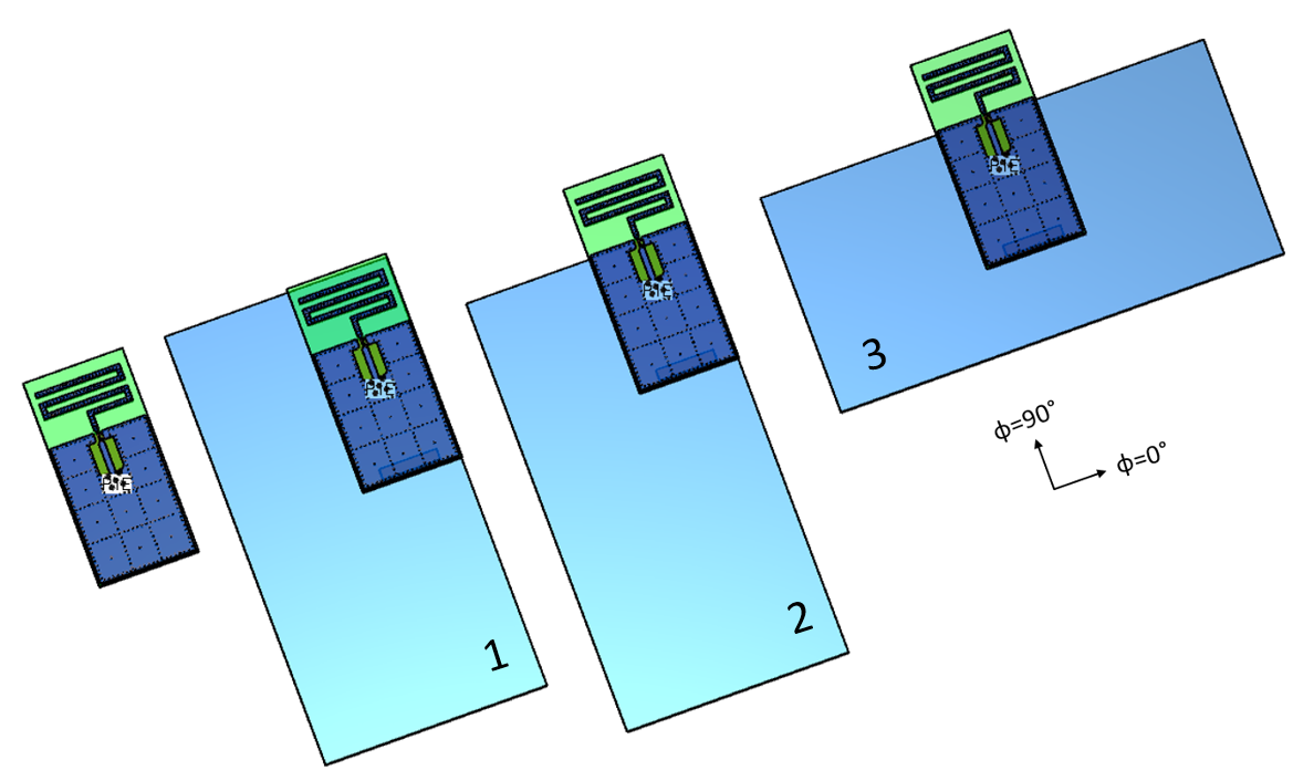
For position 1, with the RF board overlapping the motherboard, the antenna fails completely. VSWR is >100 which means almost total reflection in this environment. Perfect radio board, but wrong placement.
For better performance, we move the radio board so that the entire antenna area is clear from any PCB traces below. This position 2, on the edge of the motherboard, results in some de-tuning of the resonance frequency and VSWR = 5 at 868 MHz. With the antenna at the center of the PCB at position 3, we find a stronger frequency shift and VSWR = 10 at 868 MHz.
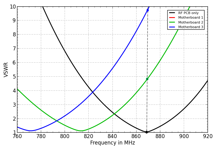
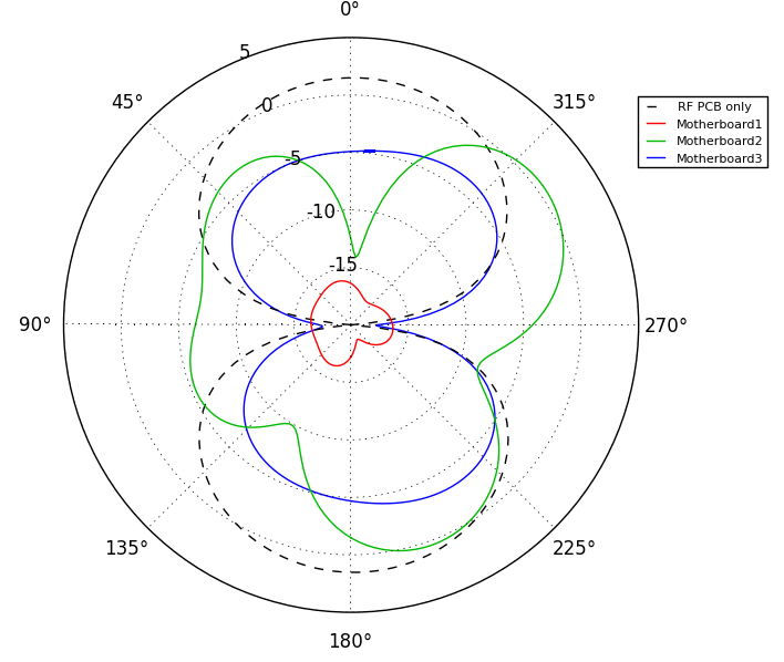
Remember, we started from a radio board that was tuned perfectly to VSWR=1 at 868 MHz. The only change was mounting the radio board to a motherboard. This results not only in a strong resonance shift, we also observe a change in antenna pattern.
The worst result (red) is with the antenna overlapping the motherboard: realized antenna gain -16dBi and less. For position 3, the antenna centered on one side, we see a dipole-like “8” shape similar to the stand-alone RF module. The only difference is the -6dB reduction in realized gain due to mismatch. For position 2, the antenna at the edge of the motherboard, we see a more omnidirectional coverage, but one minimum at phi=0° where the stand-alone RF board had a radiation maximum.
It is quite obvious from this example that placement and environment matters. We can’t expect good system performance without taking the interaction of antenna and motherboard into account.
EM simulation enables us to design for a real world antenna environment early on. It also enables us to study material tolerances and select the right PCB material for the job, with the required tolerances.
Design for an environment
Next, we investigate a small 868MHz antenna for a USB-size device [2]. This small form factor means the built-in ground is small, and whatever ground is connected to the USB stick becomes part of the overall antenna design. Tuning such an antenna for stand alone operation of the USB stick is not appropriate, as we will see.
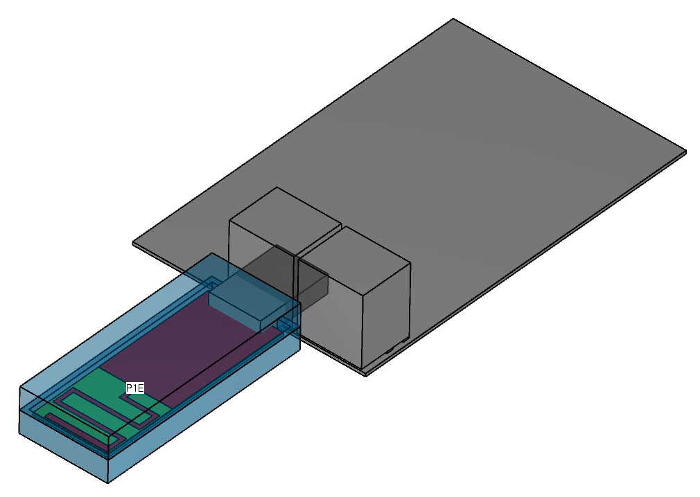
The antenna is tuned for operation with a Raspberry Pi board connected to USB ground. This environment significantly increases the effective ground size, and has a strong impact on antenna matching and radiation efficiency.
The red curve in the VSWR plot below represents the antenna response for the stick connected to the Raspberry Pi. The black curve shows the stick stand-alone: much different in impedance and resonance frequency.
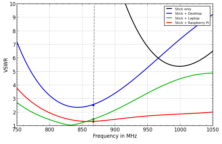
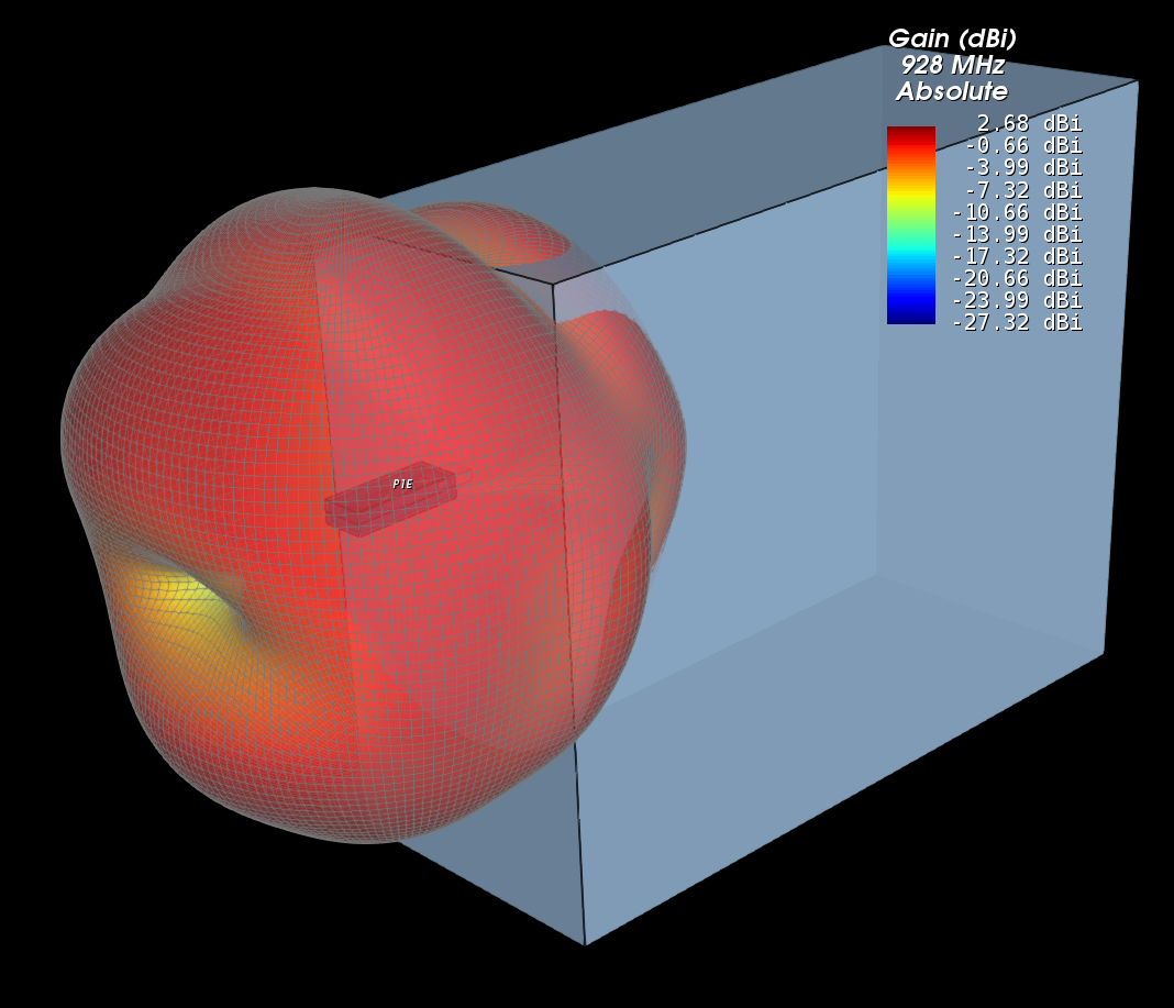
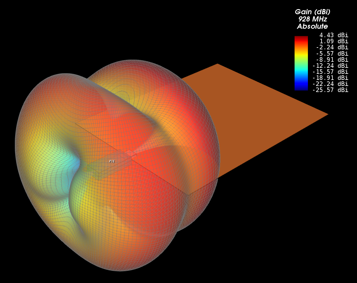
However, with the antenna design optimized for the Raspi environment, other environments like the laptop or desktop PC-like environment can be used with very reasonable VSWR! The resulting antenna patterns can be obtained easily from EM simulation.

2.4 GHz antenna placement on board edge
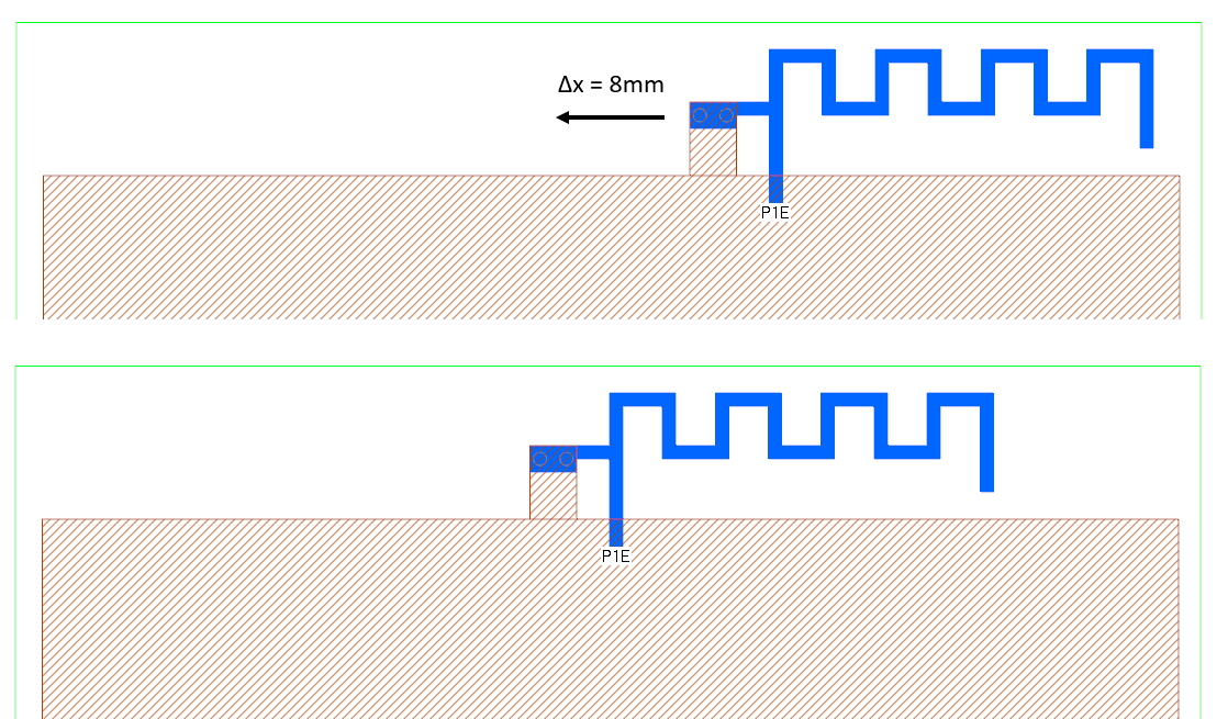
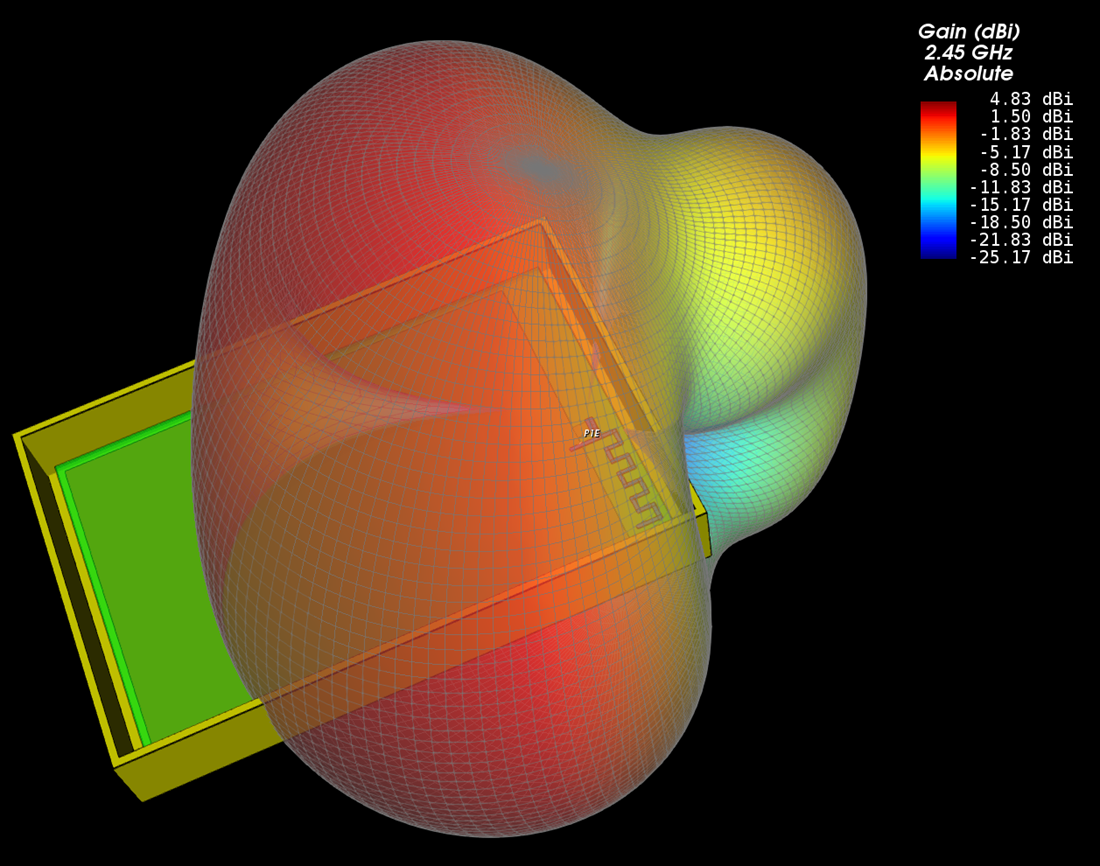
Next, the placement of a meandered F-antenna at 2.4 GHz is investigated [3]. Starting from a baseline placement near the PCB corner, the antenna is shifted to the left by 4mm and 8mm.
The antenna itself is rather narrow band, because the radiator is close to the PCB ground. This means that even moderate resonance shift cause a relevant mismatch loss.
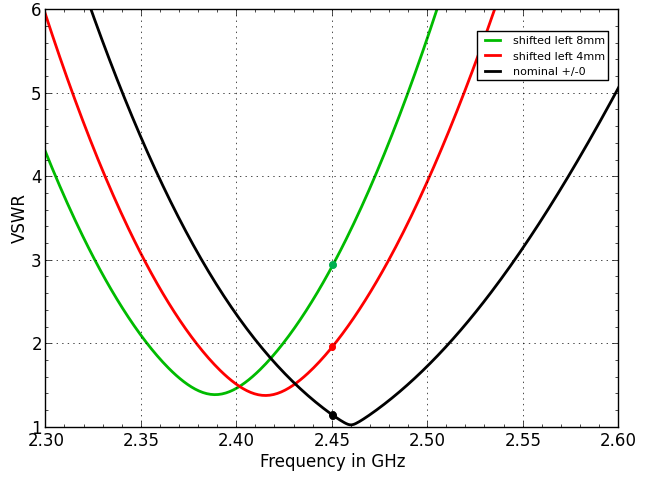
The small shift of 8mm to the left causes an increase of VSWR from 1.2 to 3, and some minor change in radiation pattern. In the lab, such a resonance shift could be compensated by tweaking the antenna length.
Simulate or measure? Simulate and measure!
So how should we design and optimize our antennas? Is a design from 3rd party appnotes with some post-layout tuning in the lab sufficient, or do we really need EM simulation?
For small antennas, where every small change to the layout changes the entire antenna behaviour, an experimental design is rather difficult: just by attaching the network analyzer’s coax cable to the device, we have already changed the ground situation and antenna response. Optimizing the VNA response can be misleading in this case, and doesn’t provide best performance and range in real world operation. In such cases, a simulation-assisted design is very important, to understand external influences and develop a tuning strategy. Based on a good understanding from simulation, fine tuning the details in the lab is easy.
Using this EM-simulation assisted methodology, the author was able to significantly improve the range of a 868/915 MHz USB radio stick, at reduced cost compared to previous antenna designs.
EM-assisted antenna design is also useful for application with uncertain environment, such as IoT devices or wall mounted Smart Home devices. The actual operating environment of these devices isn’t know at design time, so it is mandatory to design a robust antenna that can tolerate external influences. EM simulation is an important tool in this case.
For antennas with a large ground, well defined placement and fixed environment, some experimental post-layout tuning can be sufficient. But even for these cases, an EM simulation based tuning strategy can help to speed up the design process.
Summary
For best possible range and antenna performance, designers can take advantage of EM simulation early on during the design phase.
For small antennas that are very sensitive to external influences, EM simulation enables the antenna designer to account for the actual PCB dimensions and expected antenna environment.
For any PCB antenna, EM simulation enables the antenna designer to account for material tolerances and design a more robust antenna that performs well not only in the lab, but also in mass production and real world environments.
References and simulation models
[1] http://www.ti.com/lit/an/swra227e/swra227e.pdf
[2] Empire XPU simulation model download: USB-stick 868 MHz with Raspi
[3] Empire XPU simulation model download: 2.4 GHz antenna parameter sweep
[4] 3D EM simulation using Empire XPU
If you are interested in EM simulation tools or services for your antenna design, please do not hesitate to contact us.
Customers in Germany, please find us at antennensimulation.de