
In the previous simulation report, we had a look at the dual antenna version ESP32-WROOM-DA, with some assumptions on the ground layout used in that module. In this report, we will look at the influence of motherboard size, and the famous “keepout” area if we place the module “inside” the PCB.
Single antenna case – ESP32-WROOM-32E
Let’s start with the single antenna layout. Simulation is done for motherboard sizes from 25mm x 25mm to 100mm x 100m. Click the picture for full size view.
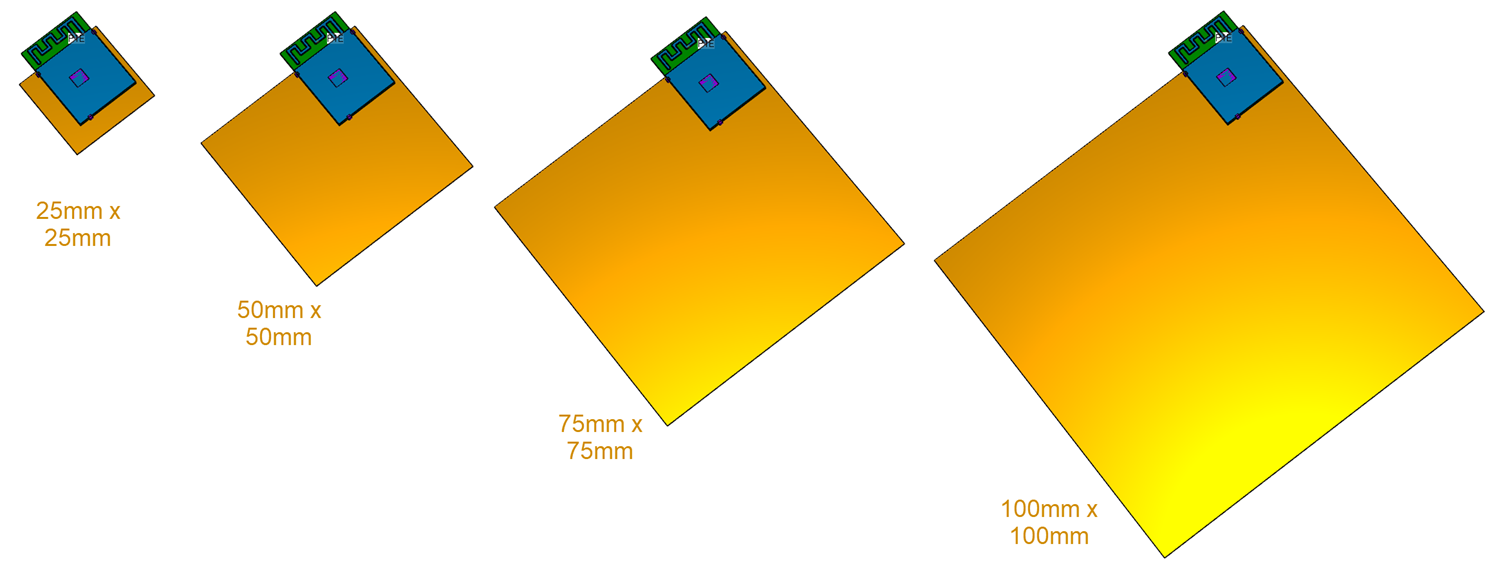
We find that motherboard size of 50mm x 50mm and above provide good VSWR, if the antenna is mounted in the corner as documented in the Hardware Design Guidelines.
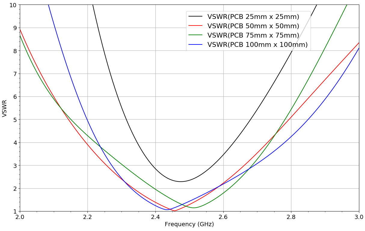
Antenna pattern varies with ground size: small PCB size has a more omnidirectional pattern, whereas larger PCB show some dips in the pattern. That’s why the dual antenna version was invented, to enable antenna diversity switching.
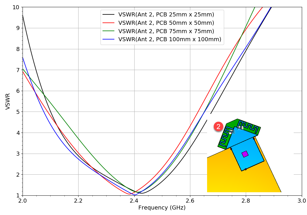
Dual antenna case – ESP32-WROOM-DA
The next model is the dual antenna version, as a best-guess based on the photo in the press release. Note that the actual product might use slightly different layout, actual PCB layouts were not yet available when this report was created.
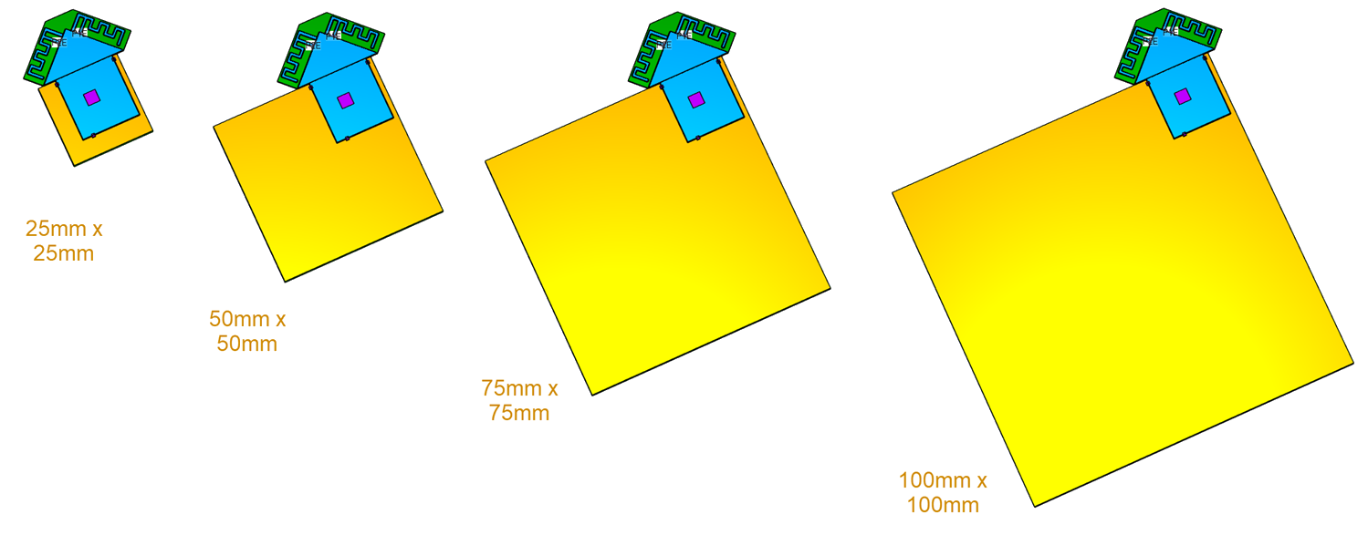
It is no suprise that VSWR of both antennas is slightly different, because the local ground situation is different: the right antenna (1) has its “hot” end of the radiator at the PCB corner, while for the left antenna (2) that is located away from the corner. However, we did not expect different sensitivity to the motherboard size:
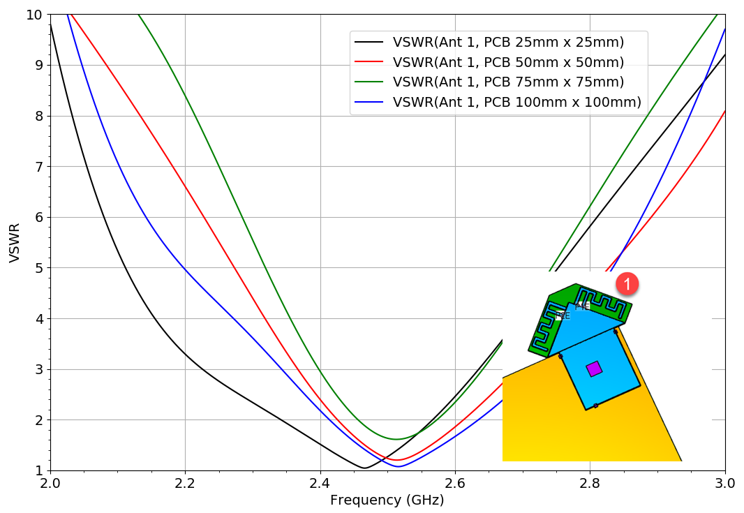
The antenna that is located away from the edge (here called antenna 2) is almost insensitive to all PCB sizes tested here, including the small 25mm x 25mm board. That was not expected!
For that smallest motherboard, placement approaches the symmetric case where both antennas have the same distance to the nearest corner. As as sanity check, that testcase with 21mm x 21mm motherboard size is done:
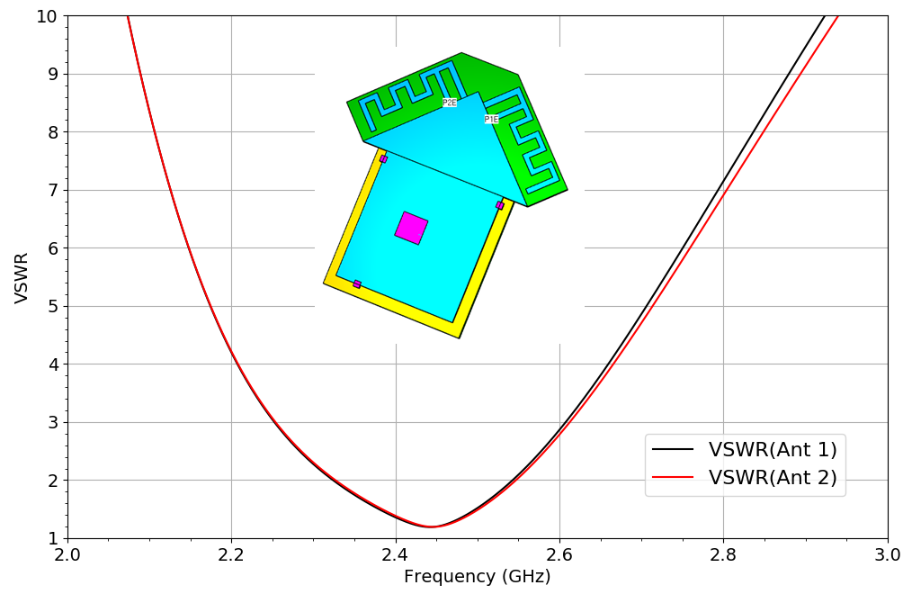
So indeed, the antenna closer to the PCB corner is a bit more sensitive to motherboard size.
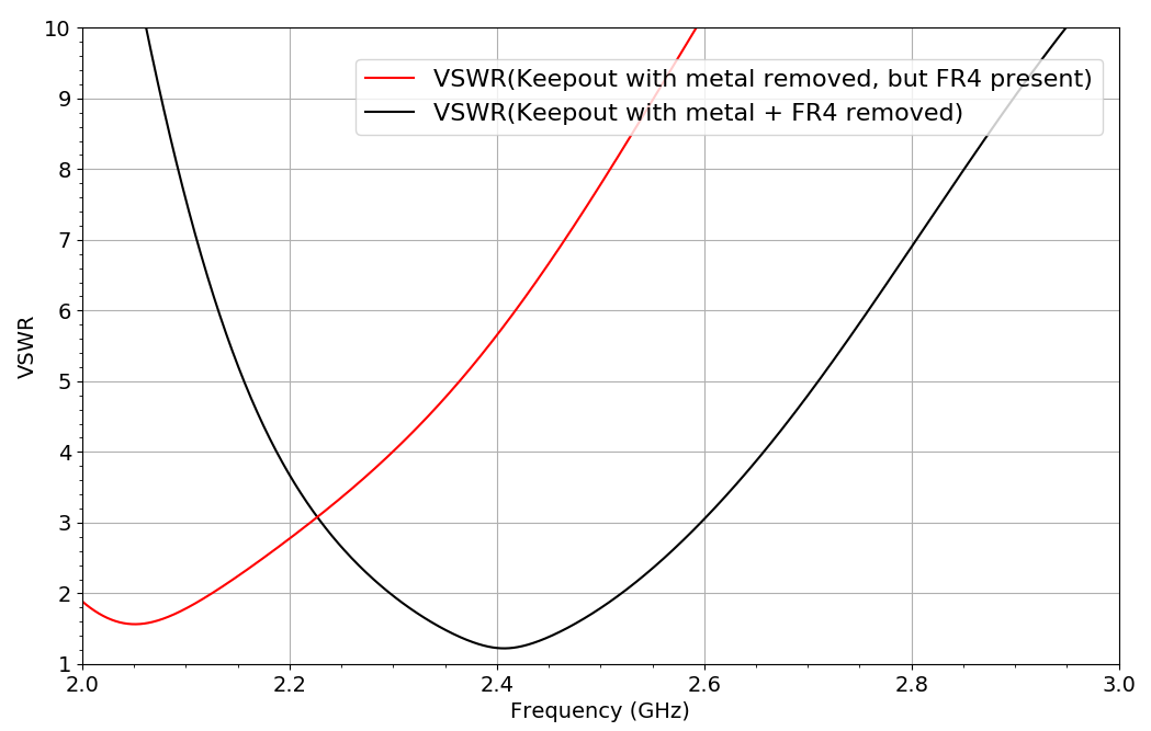
Keepout area
In the Hardware Design Guidelines chapter 3.1.2, a keepout area of 15mm around the antenna region is recommended when the module is placed “inside” the main board. It says “The antenna area of the module and the area 15 mm outside the antenna should be kept clean, (namely nocopper, routing, components on it)“ but does not really discuss the PCB dielectric material. Let’s have a look at that!

Simulation results are very clear on this: there must be no PCB material underneath the ESP32 antenna! It is not sufficient to keep out metal/traces/ground, the FR4 material itself will tune the antenna to lower frequencies. That is no different from de-tuning the antenna by inapproriate boxing that is too close to the antenna.
3D EM simulations above were done using Empire XPU, a very fast and efficient simulation tool based on FDTD method. As a value-added Empire reseller, we can provide simulation models and evaluation software on request. We also provide consulting services for antenna design and simulation-based optimization of antennas for your specific environment, which might be less ideal than the reference PCB discussed here. We can support you for cases where reference designs fail.
Interested? Please get in touch!