
In this application note, we will use Empire XPU simulation with time domain results for pulse excitation to understand and optimize the transition from chip to PCB. This method gives detailed insight on the location of discontinuities along the signal path.
Readers who have used Time Domain Reflectometry (TDR) will be familiar with this analysis method: use a pulse excitation to study reflected and transmitted voltage vs. time, while the pulse is travelling along the signal path. At any discontinuity, amplitude and sign of the reflected signal tell us about the change in line impedance. The spatial resolution depends on the bandwidth of the pulse.
A simple RFIC model is used for demonstration, based on IHP SG13S stackup. The main purpose of this application note is to show the analysis workflow – the design example is only a quick testcase and not a real circuit. TSV size in this example is larger than actual TSV in SG13S technology.
The test circuit
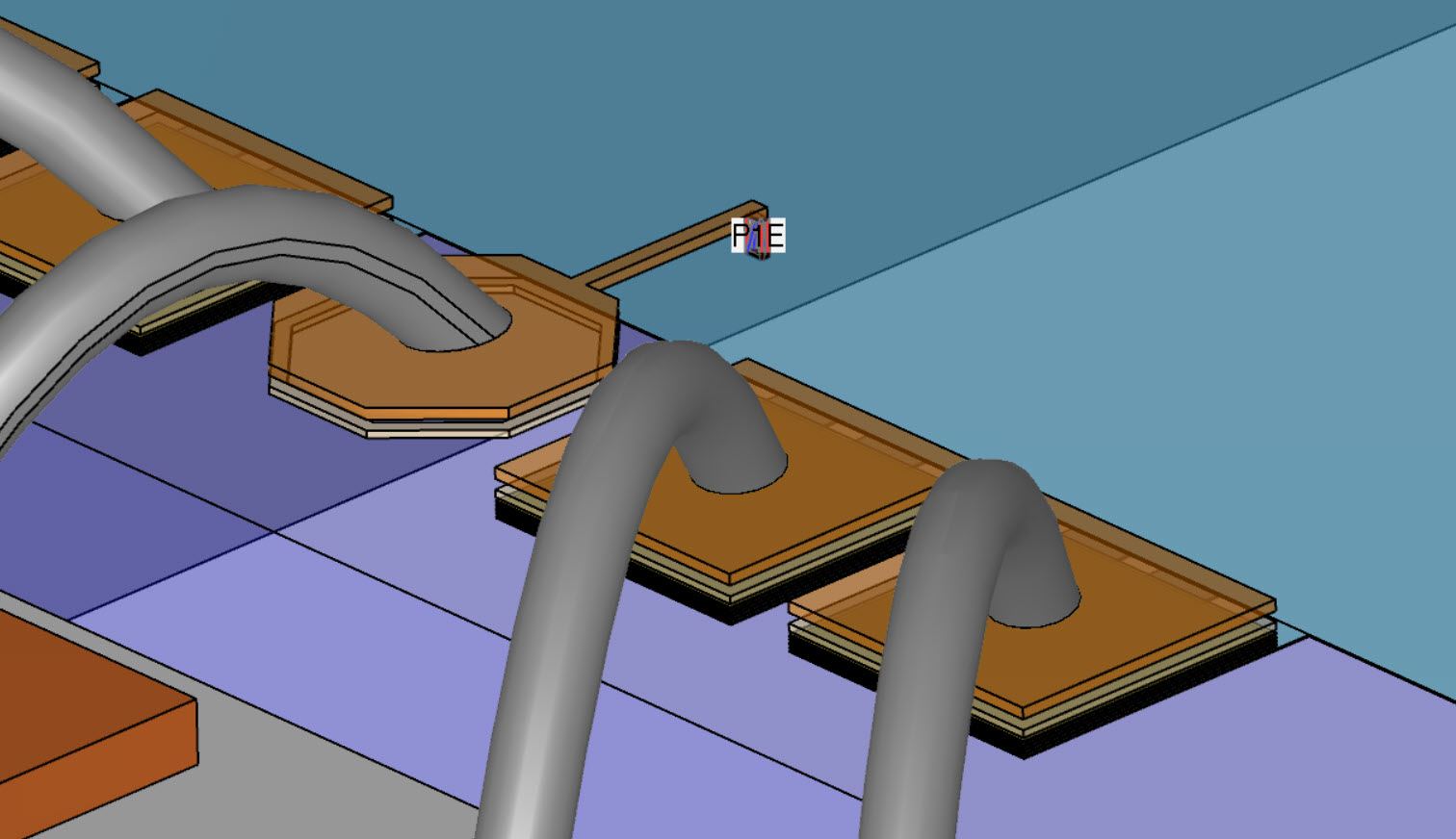
Baseline model for this appnote is a 300µm thick chip placed inside a recessed cutout of the 254µm PCB, to minimize interconnect length. Wire bonds are used to connect the RF line as well as the multiple grounds. Pad size for the ground pads is 80µm with 20µm spacing.
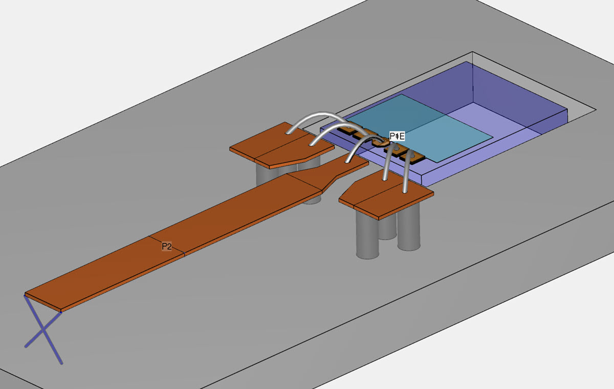
On chip, a lumped vertical port from TopMetal2 to Metal1 is used. The blue RF ground polygon on Metal 1 is approx. 10µm below the pads, so we have a nice short connection to all signal and ground pads. (Note to the GaAs designers: this SiGe stackup is different from GaAs, we don’t have the chip backside as the RF ground.)
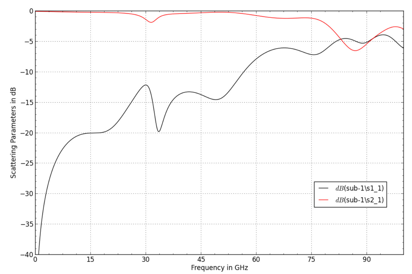
This results in rather poor RF performance as shown below:
Now the question is: what are the reasons for this poor matching, is it just the bond wire inductance? How to improve the response? This is where time domain results for pulse excitation are useful, to localized the discontinuities.
Test circuit time analyzed with time domain pulse
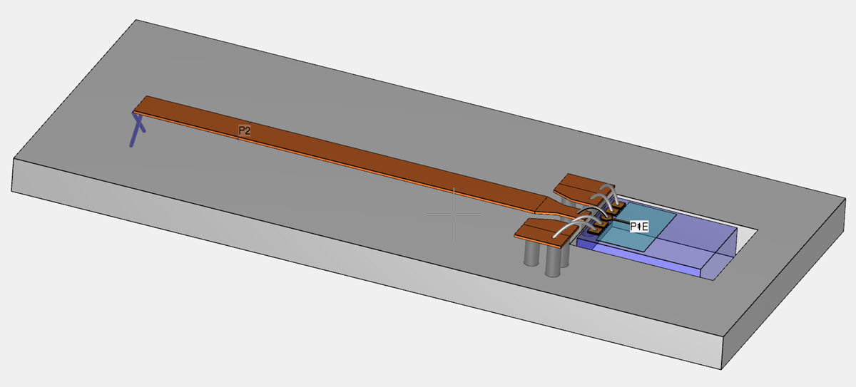
To help with an initial understanding of the time domain results, we have stretched the microstrip line on PCB. This results in a longer time delay until the signal from the chip reaches port 2 on the PCB, and we can study the reflections from the interconnect more easily.
For excitation at port 1 on chip, we use a square pulse with 5ps duration, instead of the default gaussian pulse that is used for S-parameter simulations.
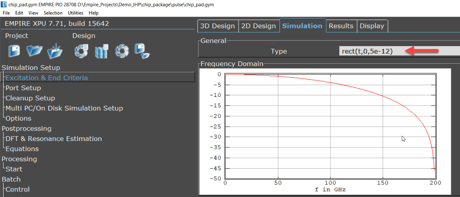
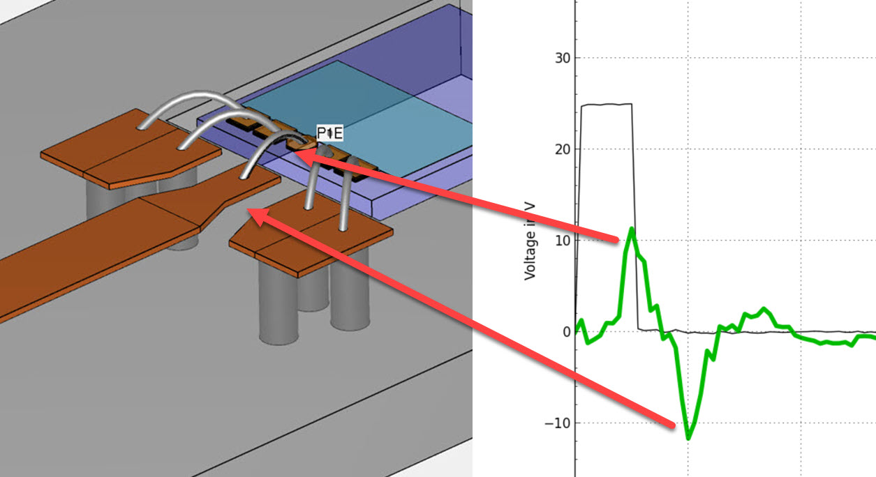
Simulation results for the time domain signal are shown below, plotted over time. Red is the incident voltage that we have defined in the excitation, green is the reflected voltage, black is the total instantaneous voltage at port 1 (incident + reflected) and blue is the voltage at port 2. We can see the time delay of the transmission of around 28ps, with a low pass response that takes out the fast slope from our initial square signal.

The green curve shows a positive reflection (line impedance increase) at 5ps delay and a negative reflection (line impedance decrease) at 10ps delay. This is the main issue that we need to solve. Looking at the geometry and related electrical length, we can identify that the positive peak is the bond wire (too much series inductance) and the negative peak is the pad at the end of the bond wire on PCB (too much shunt capacitance between signal and ground).
Improving the layout
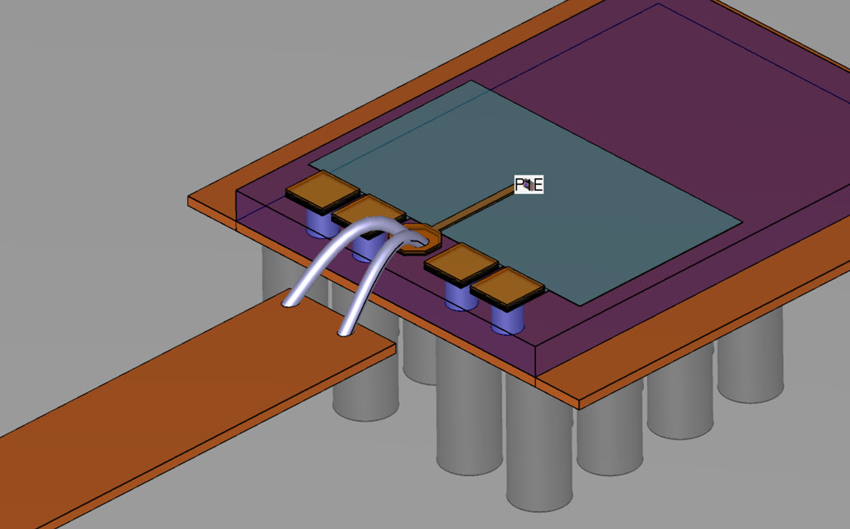
Now that we have identified these two issues, we can think about counter measures: by changing the ground connection from wire bond to TSV, we can get rid of the ground pads that are near the signal pad on PCB. This reduces the shunt capacitance between signal and ground. It also enables us to increase signal line width at the bond (with having extra capacitance from small gap) and then have two bond wires for the signal path, instead of one.
TSV require a reduced chip thickness of 75µm, so the chip is now placed onto the PCB top side, without recessed mounting.
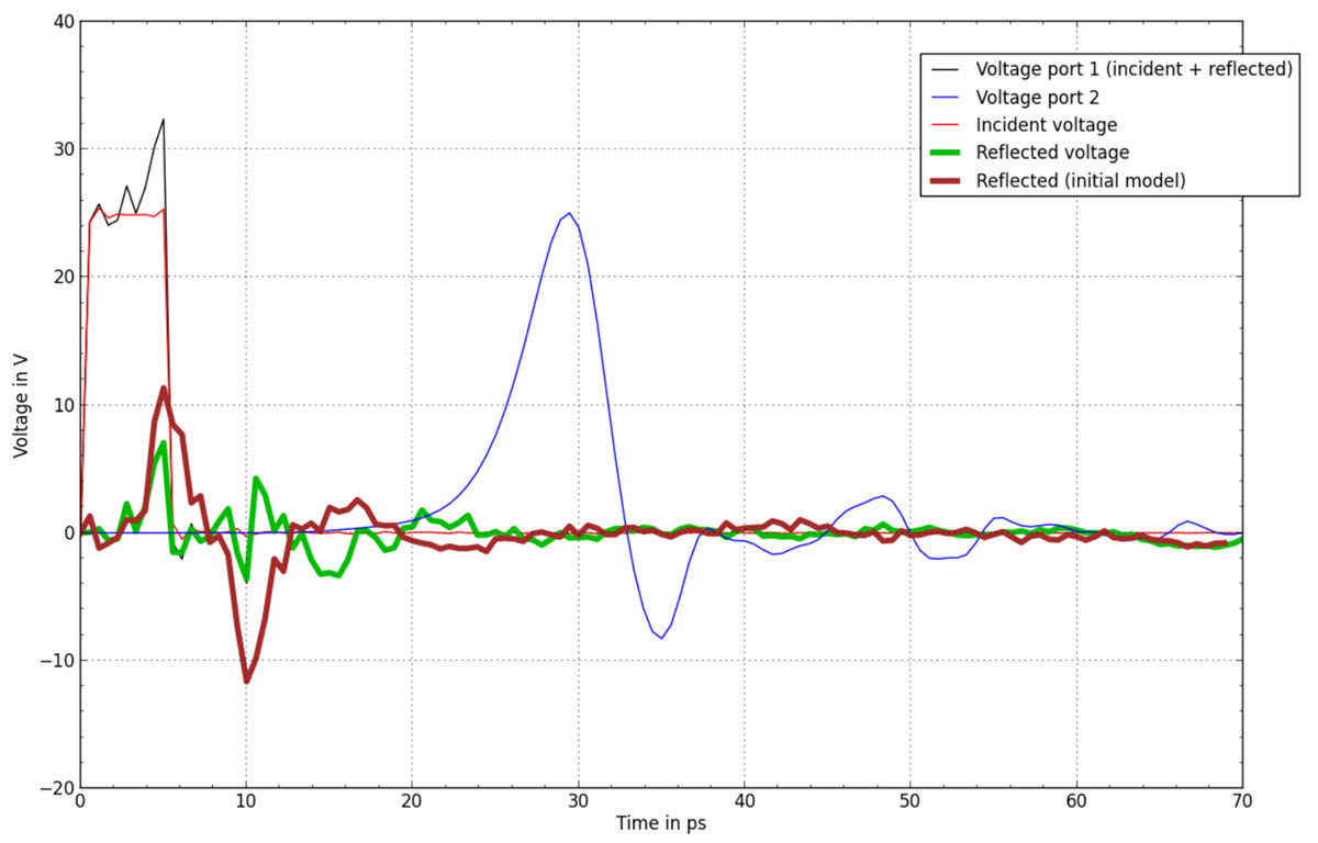
In time domain, we can see a strong reduction of the reflected signal (green) compared to the previous model (brown): The positive peak from bond wire inductance is much reduced, and the negative peak from the excess capacitance at the PCB landing pad is almost gone. So we expect a much better wideband performance now.
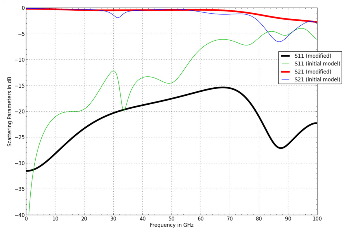
When evaluating the model for S-parameters, this is indeed confirmed, with much better return loss at higher frequencies:
Why use time domain EM simulation?
Here, we use a time domain EM solver (Empire XPU) with direct pulse excitation in the time domain. This enables EM simulation with very short pulses, resulting in very high spatial resolution of discontinuities.
An alternative method would be EM simulation in the frequency domain (FEM or MoM) where S-parameters are simulated first, and time domain analysis is done by fourier transform of the S-parameters. In that case, we would need very wideband S-parameters to realize such short pulses (5ps pulse with <1ps rise time) for high spatial resolution.
Summary
In this appnote, we have seen how TDR-like simulation methods, with evaluation of pulses in the time domain, can help to improve wide band response of interconnects. This type of simulation is easily done in Empire XPU by switching from the default gaussian excitation (useful for S-parameter simulation) to user defined excitation. Simulation times are very short using this method, because the FDTD method uses direct simulation in the time domain. Simulation time was less than 3 minutes on a Core i9 desktop PC, using 3 million mesh cells.
If needed, a more complex time signal could also be used for simulation, or an excitation signal with controlled rise time. However, for this “computed TDR” analysis the fast square wave signal seemed most useful.
Click here for more information on Empire XPU