This application note describes on-chip antenna modelling with Empire 3D EM.
The antenna design in this appnote is based on: K. Schmalz, W. Ruoyu, J. Borngräber, W. Debski, W. Winkler , and C.Meliani, “245 GHz SiGe transmitter with integrated antenna and external PLL,” in IEEE IMS, 2013, pp. 1–3.
Drawings with antenna dimensions can also be found here on pages 80-82.
Simulation model
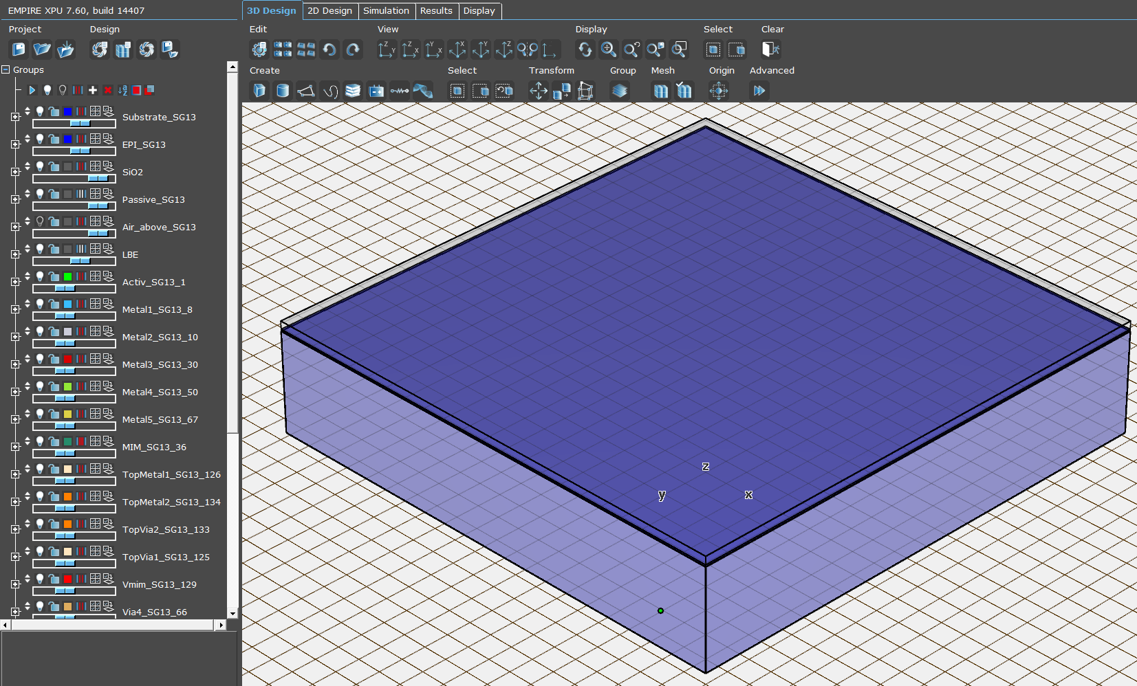
First, an empty simulation model was created using the Empire template for IHP SG13S/SG13G2 technology with substrate thickness set to 200µm. This template creates an empty model with all metal, via and dielectric materials already predefined, with the correct position and height and material properties.
For the antenna, geometries were then drawn in the Empire 2D editor, based on dimensions given in the paper. The size of Metal1 ground plane and some feed line dimensions are not specified there, so these dimensions are an educated guess.
Localized backside etching (LBE) underneath the antennas can be modelled in two ways: by drawing a rectangle on the LBE layer, or by cutting out a rectangle from the existing boxes on layers Substrate and EPI. The easier method is to draw the LBE area on the LBE layer (=air), which has higher priority for the simulator than Substrate and EPI, so that it effectively removes the silicon during simulation and places an air box instead. However, for this application note we have created cutouts to Substrate and EPI layers using boolean operations, because that gives the nicer pictures in 3D view ;-)
For the antenna feed, a perpendicular port from TopMetal2 to Metal1 was created.
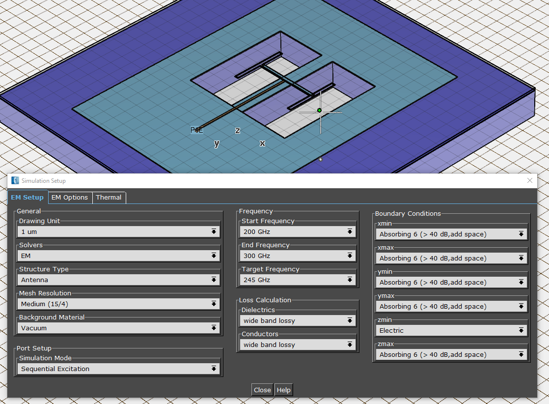
The structure type was changed to “antenna”. To ensure good absorbtion at the boundaries at any angle, boundary conditions were changed from absorbing sheet (= template default for structures with little radiation) to perfectly matched layer (PML) with 6 sheets and automatic distance from the drawn structure. Only at the bottom of the model, an electric boundary was used to represent the “module ground plane” described in the paper.
Boundary distance and mesh
The screenshot below shows the simulation model with actual boundaries, with 325µm space added automatically between the drawn structures and the boundaries:
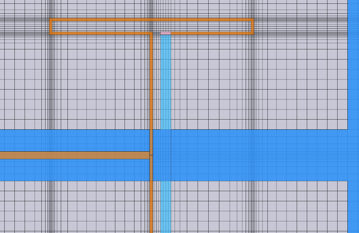
For good accuracy, medium mesh settings were used with 15 cells/wavelength and a minimum of 5 cells for the conductor width.
This results in a total of 1.8M mesh cells net (2.5M cells including PML6 boundaries), with minimum cell size of 0.4µm in vertical direction.
Far field recording
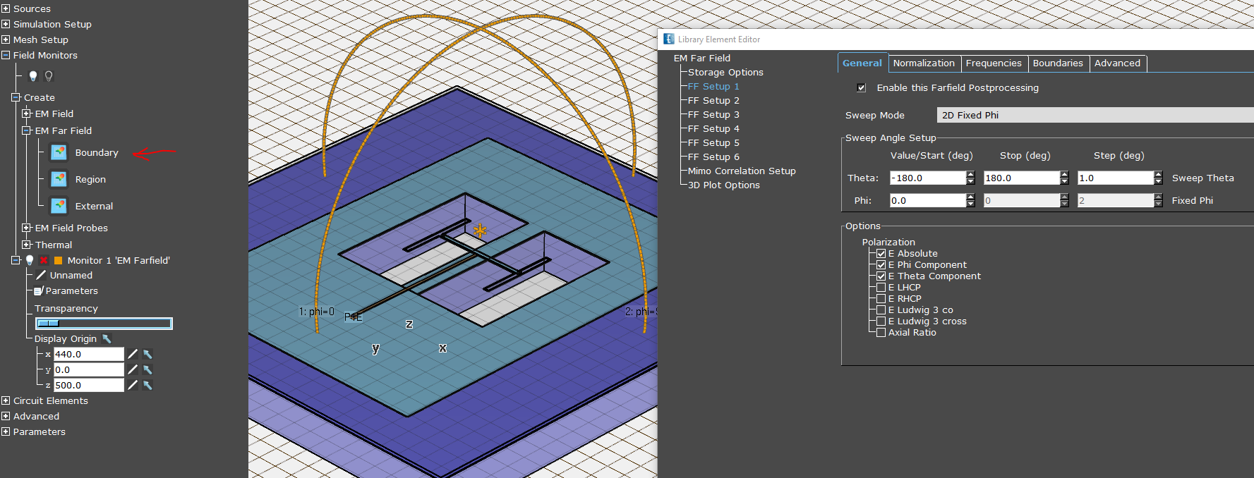
For antenna parameter calculation, a Field Monitor of type EM Far Field: Boundary was created. This samples the field at the outer boundary of the model. Therein, FF Setup 1 to 4 were enabled: far field for fixed phi=0°, phi=90°, both angles sweept for 3D pattern display, and finally the gain at theta=0, phi=0 for antenna gain plot over frequency.
For all these parameters, normalization was changed from “directivity” to “gain”.
In the 3D editor, the orientation of selected far field cuts is shown when the field monitor is enabled.
Simulation time
Simulation time is 2m:20s for the full frequency range 200 – 300 GHz on a Core i9-7940X desktop computer. Model size is 1.8M mesh cells for geometries, or 2.5M mesh cells total including the PML6 boundaries.
Antenna matching
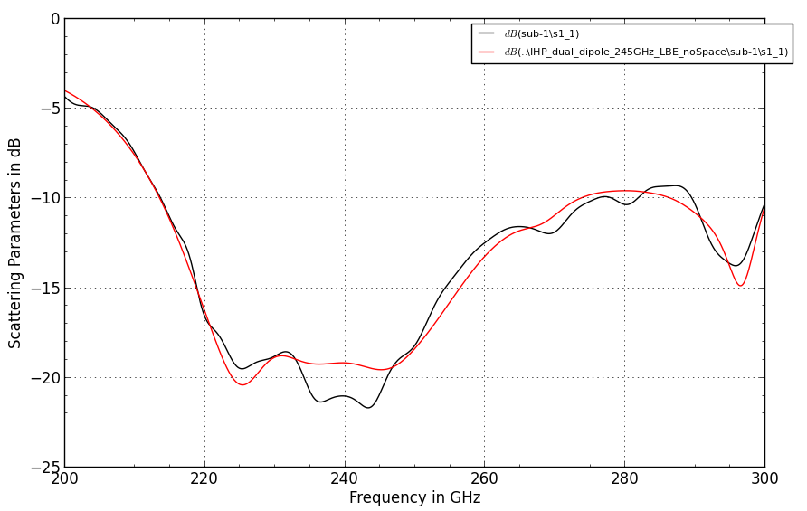
In the plot below, the black curve shows the input matching from 200-300 GHz. The ripple is a true physical effect, caused by internal reflections in the silicon substrate, and depends on the substrate size. It is seen here because the absorbing side boundaries are placed at 1/4 wavelength distance from the substrate, and don’t attenuate the substrate resonance.
If we place the absorbing side boundaries directly at the substrate, that ripple disappears, as shown by the red curve. If we are interested in the actual ripple for a given chip size, the substrate size needs to be modelled accordingly.
Antenna gain and radiation efficiency
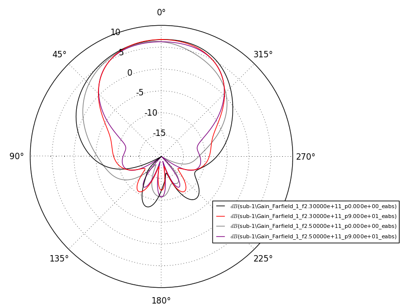
The antenna gain (abs) for phi=0° and phi=90° is shown in the plot below for 230 GHz and 250 GHz. This agrees well with the 7dB gain mentioned in the reference.
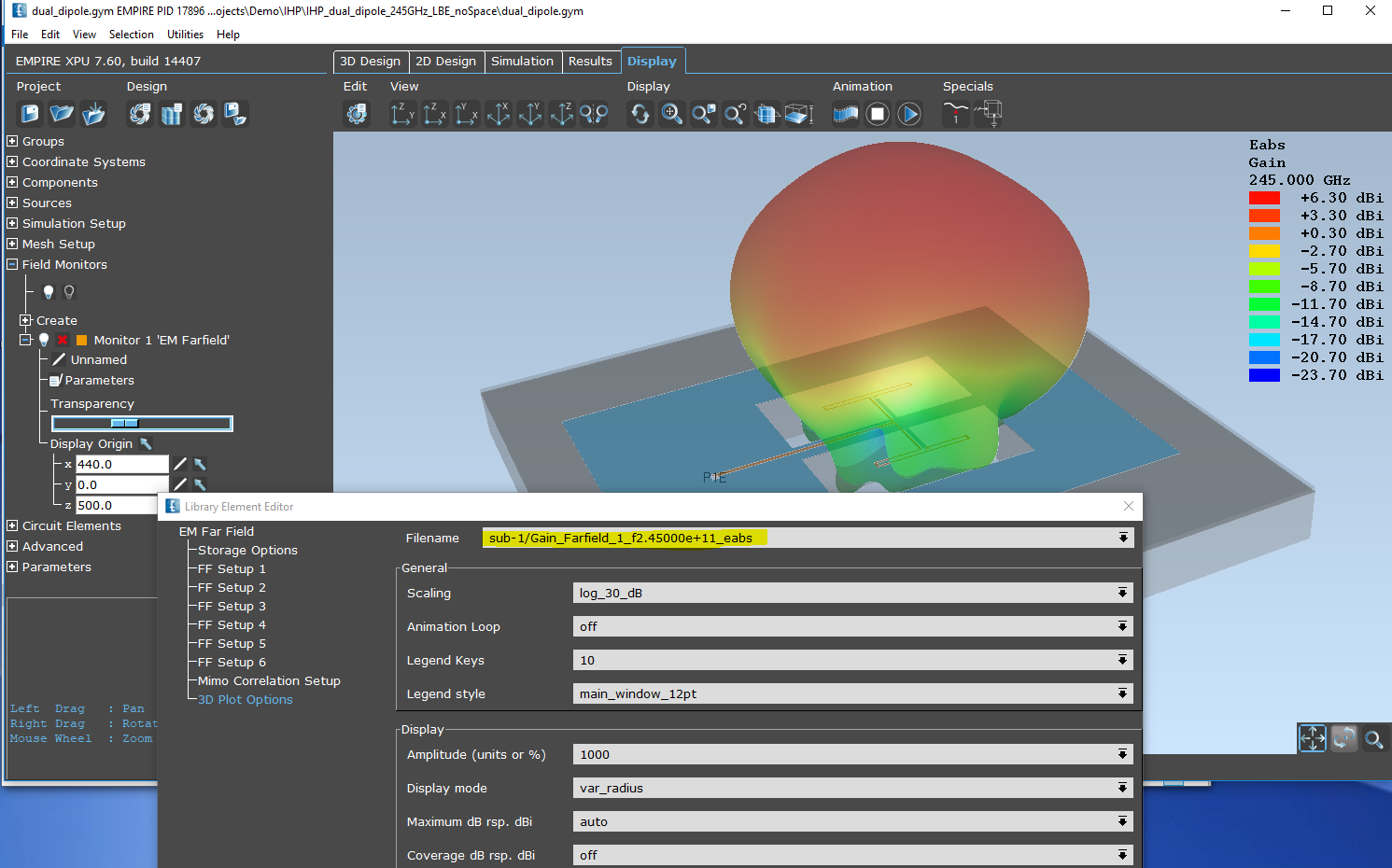
Visualization of the antenna pattern is also available as a 3D plot. If the far field is recorded for multiple frequencies, the data set for display can be chosen:
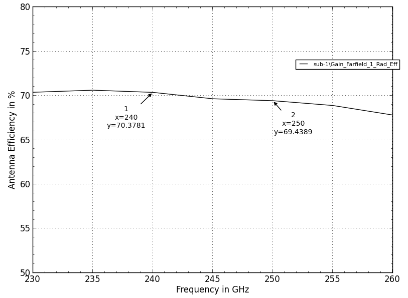
For each far field calculation, the antenna efficiency is calculated from the total radiated power and the input power into the antenna. This is available in results window as “nu(f) Antenna Efficiency”).
This ends our application note on simulation of an RFIC on-chip antenna in IHP SG13S/SG13G2 technology. For more information on the SG13S template for Empire XPU, have a look here. For more information on Empire XPU meshing for RFIC simulations, have a look here.


