
This application report describes EM simulation of a 165 Ghz on-chip antenna in Empire XPU and compares results to measurements.
The antenna design was created by Wael A. Ahmad (IHP) et al. Design and antenna simulation results using FEM simulation are published here: https://ieeexplore.ieee.org/document/8827282
In the original paper, FEM simulations “with filler” are approximated as solid metal planes. Here in this application report, we here study a much more detailed model, with all that complex patterned structure, and even the complete large (but finite) PCB ground plane underneath the chip.
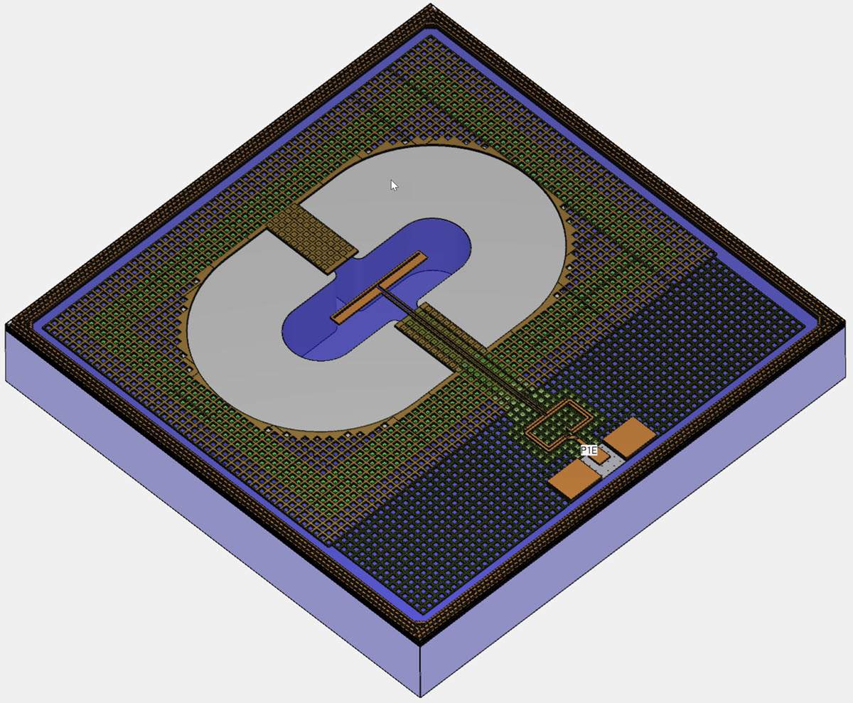
Simulation “chip only”, detailed geometry model
As a starting point, the antenna chip was simulated with an ideal backside metalization. Later, we will study the additional effects of the 50mm x 50mm PCB on the antenna pattern in a separate model.
For simulation, vias on the upper metal layers and fillers are included with full detail, only the lower vias are merged. This results in a model with more than 200,000 objects. Automatic meshing was used, but mesh in x and y direction was limited to 0.42µm which corresponds to the size of the medium size vias. Resulting model size was 58 Million mesh cells, and requires only 3 GB of RAM because of the memory-efficient FDTD method.
Below are some screenshots showing the amount of detail modelled in this EM model, at different zoom levels:
 The curved boundary in localized backside etching was modelled based on the chip photo, instead of the ideal dimensions from the GDSII file.
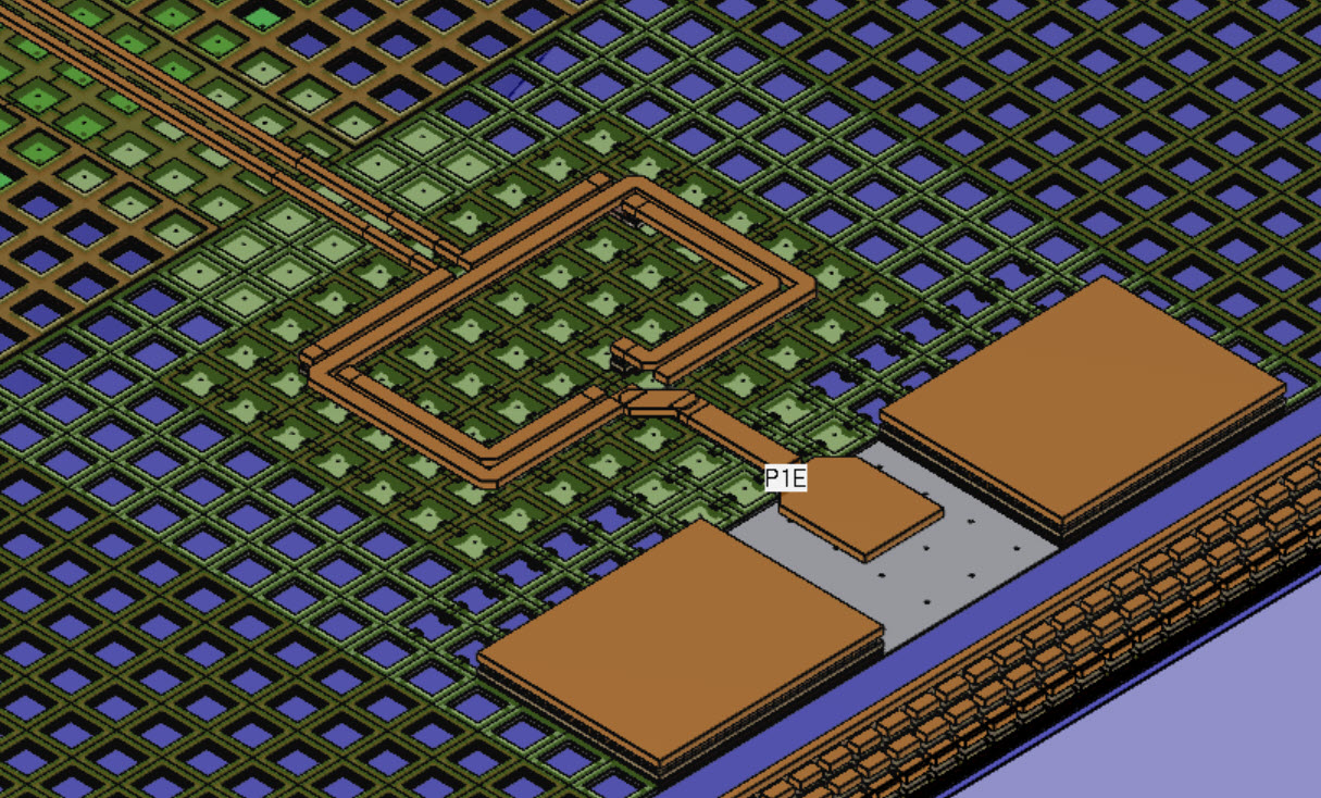 The antenna model includes the balun used to create a differential signal from the single ended feed. For exciation, a lumped port was used between TopMetal2 and the ground plane.
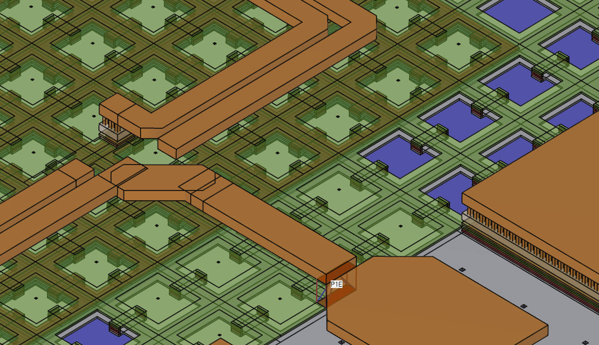 The mesh resolution of up to 0.42µm is enough to resolve all individual vias (0.9µm via size) in the array shown below, as well as the small 0.5µm cutouts in the ground metal.

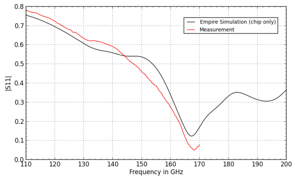
Comparison of measurement and chip-only simulation
With the simulation model show above, using the actual backside etch shape as measured from the chip photo, we get a frequency response that is close to measurement. For frequencies above 170 GHz, no measurements are available for S11.
Next, we compare the antenna gain over frequency at theta=0° phi=0°:
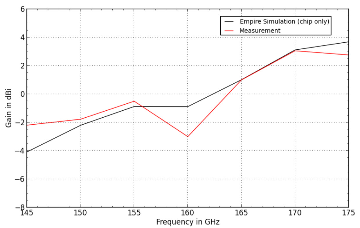
The pattern is somewhat unexpected for a dipole, with a strong signal along the dipole axis. This modified pattern results from the backside metalization and from localized backside etching with the antenna “island” over silicion.

For measurement curves, phi=0° and phi=90° are not labeled because the orientation in measurement seems to be different from what we use for simulation.

There is more ripple on the pattern in measurement, and a drop towards the horizon in both phi cuts. That is partially because of the test environment during measurement (radiation blocked by wafer prober and robot arm for rotating the setup) and partially due to the finite PCB size underneath the chip.
Let’s have a look at that effect, by including that actual PCB size in simulation!
Simulation with chip on large PCB (>30 lambda)
From measurement, a drop in gain at the horizon in both phi=0° and phi=90° direction was reported, which can be easily understood if we add the large, finite PCB ground plane underneath the chip. That ground plane size is 50 mm x 50 mm, whereas the chip itself is only 1.36 mm x 1.38mm.
We keep the chip details in our model, and add the PCB below, which results in an even more complex model.
Free space wavelength at 200 GHz is 1.5mm, so the lateral model dimensions are 33 x 33 wavelengths plus absorbing PML boundaries. This would be very challenging for FEM simulation engines. Using Empire XPU, simulation model size is 158 million cells, and requires only 7 GB of RAM because of the memory-efficient FDTD method.

Including the 33 x 33 wavelength PCB in the EM model, while keeping chip geometry details, we see that ripple in far field and the drop in gain at the horizon in both axis. To further visualize that ripple, let’s look at the 3D pattern for this finite ground size case:
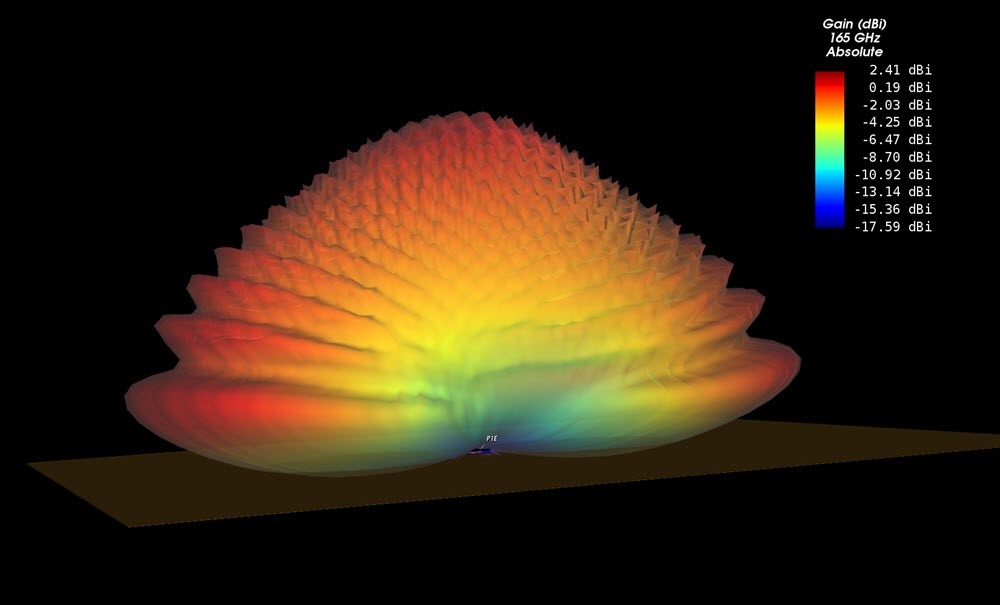
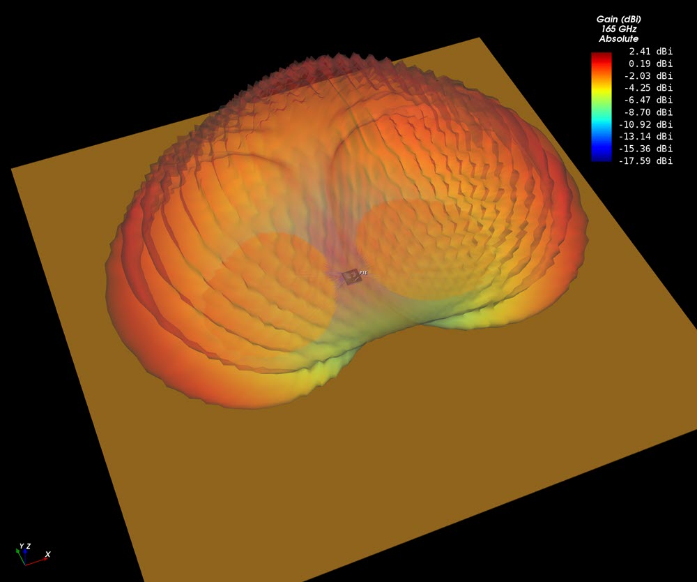
The maximum radiation (2.41dBi) is along the x-axis to an angle at slight elevation above the PCB plane, and drops at the horizon.
The finite PCB size only changes the radiation pattern. S-parameters remain unchanged in simulation, there is no practical difference between an ideal simulation ground and that large PCB.
Side note: We have modelled a chip bottom side that is perfectly touching the PCB at the bottom side, over the entire chip area. If the chip is glued onto the PCB, with a tiny air gap and only partial connection from conductive glue, that drop at the horizon (theta=90°) gets stronger.
Summary
Using Empire XPU, it was possible to simulate the complex layout with much more detail, and even include a very large PCB (>30 lambda) underneath the chip that has an influence on radiation pattern. This EM model covers an extreme range of geometry dimensions from 0.42µm (vias) to 50mm (PCB).