This is an all-new version of the transmission line pin/port application note, which also covers some new settings in ADS 2017.
When EM simulating transmission lines, port placement is simple as long as we only have a signal conductor over a large ground plane. In that case, the ground plane can be modelled as the bottom boundary of the substrate, and Momentum ports automatically place the ground reference at that nearest infinite ground plane. We only need to place a pin on the signal conductor, and Momentum knows where to connect the port reference (“minus terminal”).
It gets more complicated if we have a substrate with multiple layers and a “drawn” ground return path, instead of the infinite backside ground.
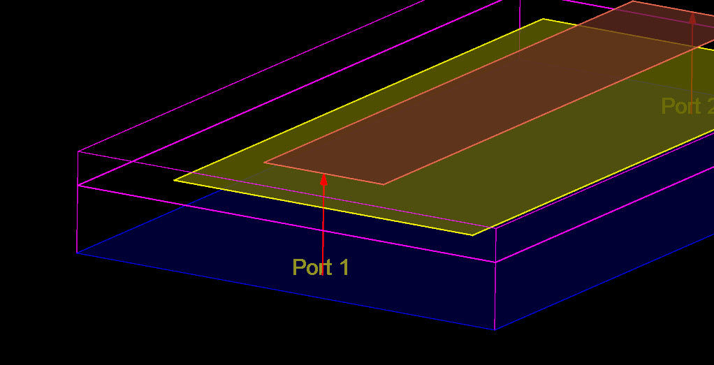
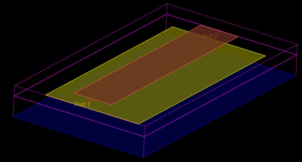
In that case, simply placing a pin on the signal conductor will still the infinite bottom ground as the return conductor, and leave the ground conductor unconnected. This can be see in the ADS 3D EM preview: ports are shown between the signal conductor and infinite ground at the bottom of the substrate.
This is wrong, because the ground conductor is floating (unconnected) and simulated return path is through the backside at the bottom of the substrate! There are multiple ways how to modify this, to obtain correct and meaningful results with the proper return path.
ADS 2017 or newer: set layer for ground reference
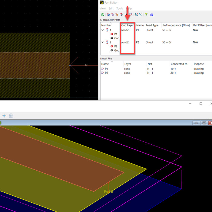
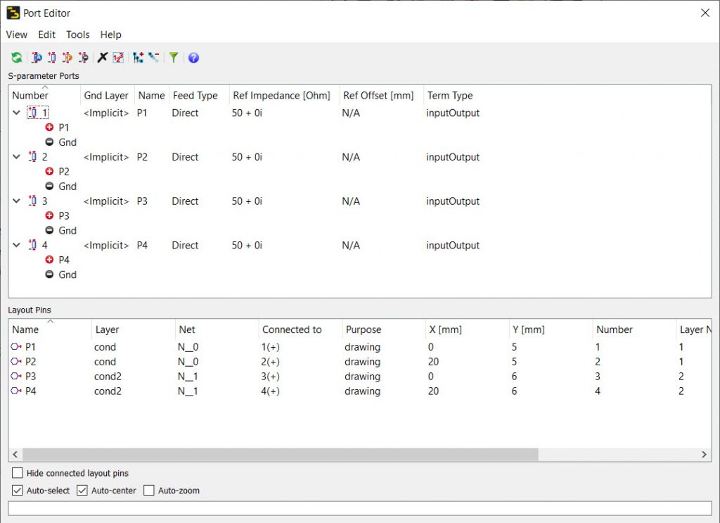
For ADS 2017 and newer, there is a new setting in the port editor that enables us to manually specify a layer for port reference, instead of using the default. Momentum will then place the port reference on that layer, assuming that a ground conductor is drawn there.
This automatically creates a differential port between two layers: the pin layer and the assigned ground layer. This is very convenient – in older ADS releases, we would need to place explicit pins for the ground reference, and tell ADS to build differential ports from the signal and the ground reference pins.
Draw explicit ground pin
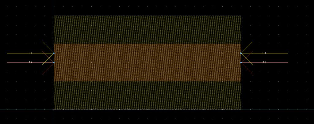
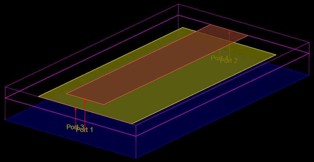
An alternative method is to manually place additional pins on the ground layer. The line will then have a total of 4 pins, 2 on each end of the line.
Here, the pins were offset a little bit for easier visualization, so that they don’t overlap. When placed on the edge of the polygon, they will extend over the entire edge of that polygon anyway, no matter where on the edge the pin is located. For more details and considerations on pin placement on a wide ground edge, see appnote on edge/area ports.
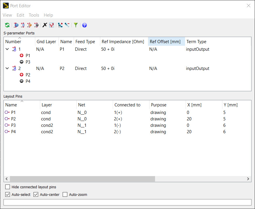
Now we have two choices what to do with the 4 pins: we can simulated this as 4 ports, or we can group the 4 pins into 2 differential ports.
Grouping of pins to one port (plus and minus) on each end of the line is done in the port editor by dragging the pin for the “minus” terminal to the port reference. For our example, this gives 2-port simulation results.
As already mentioned above: don’t worry about the “diagonal” port arrow here, Momentum will place the port over the complete edge anyway.
If we leave the 4 pins unchanged, they all use the implicit default ground, which is the infinite ground at the bottom of our substrate. Then, it is the user’s responsibility to wire this correctly in the testbench where the data is used!
What is different between these models, the 2-port with differential ports and the 4-port model?
The 2-port model has data only for one mode, that differential mode excited by the port. It does not have information on other modes, and any current flowing into the signal conductor must return through the return conductor.
The 4-port model has more data, and covers both differential and common mode use of the line, and a mixture of modes. We can use that model with current flowing through only one of the conductors, and return through the infinite backside ground. RFIC designers often prefer this model, because they can test inductance or resistance of signal and return conductor separately. But this also comes with a responsibility in using the model, as we will see later.
Just a little bit of theory: “Ports” is different from “Pins”
RF simulation tools use ports to define the source and load. While pins and ports might look similar in the layout tool, there is an important difference: a port always consists of two pins: signal and reference (“return”). The current in these two pins is the same, with opposite direction: I(signal) = – I(return). The port voltage is measured between signal and reference. In most cases, that reference is different for each port, because the ground locations are different.
In the line shown above, there is “ground” at both ends of the lines, but these two grounds are at different locations and there is some path length between them. The left “ground” is different from the right “ground”. Different locations, different potential. So instead of calling all this “ground”, we might better say “reference node of port 1” and “reference node of port 2”.
From this example, we can learn something important about what is included in the S-parameters (and what is not included). To measure the S/Y/Z-parameters of the line, at each end, we measure the port voltage between signal and ground pin, and the port current (remember? same magnitude in signal and return conductor, oppositive sign). For each port, we have one voltage and one current value.
This is the Z-matrix, which can be easily converted to the S-matrix. We will keep discussing voltages and currents, for an intuitive understanding.
V1 is the voltage (difference) between the signal pin and reference pin at port1, and V2 is the voltage (difference) between signal pin and reference pin at port 2. Only these voltages are know, with respect to these reference locations.
If we want to calculate the voltage drop on the ground conductor, between port1 reference pin and port 2 reference pin, we can’t do that. There is no such information available in our 2-port data. Take a second to realize that, it’s important.
For the 2-port simulation, we can’t separate the “signal conductor” effects from the “ground conductor” effects. If there is a gap in the line, we don’t know if the signal conductor is broken or if it is the ground conductor. Results for the 2-port simulation have all that data combined in “the line”, without separating signal and ground conductor effects.
Testbench – difference in using 2-port and 4-port results
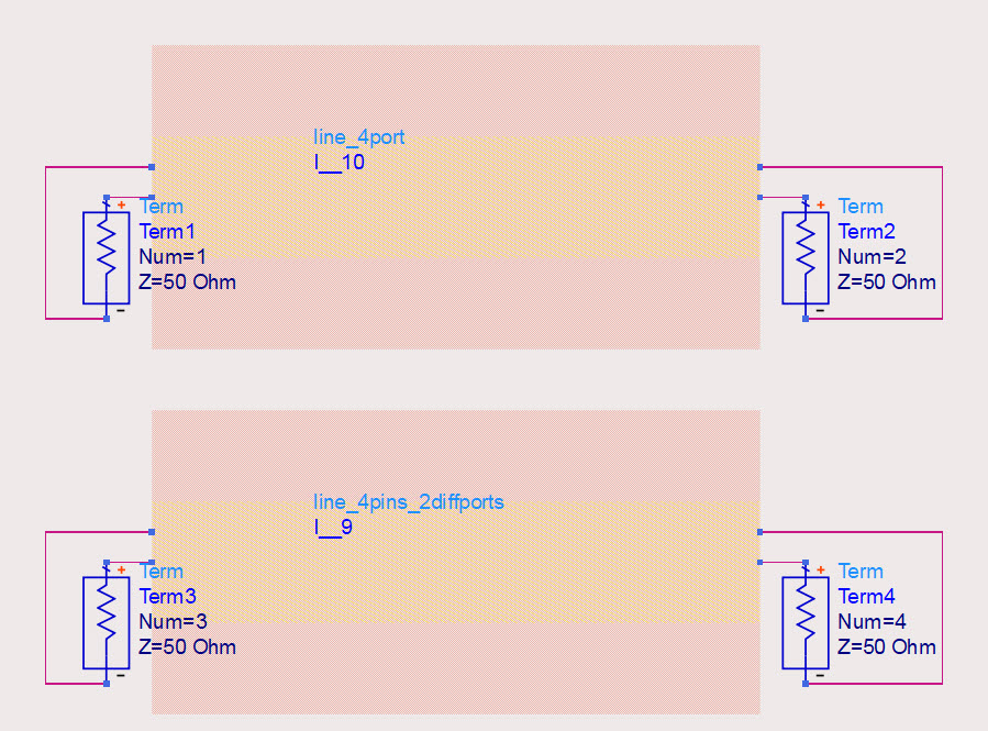
Now after we looked at that little bit of theory, let’s use line model with 2 and 4 ports in differential mode. Both are wired for differential mode, with the ADS schematic ports floating.
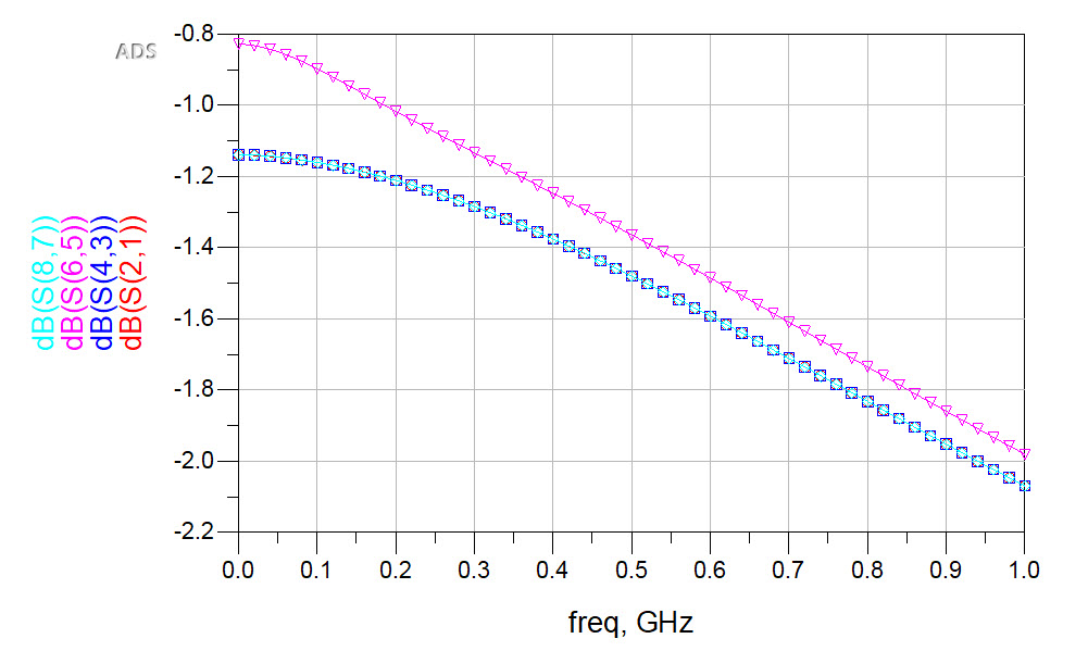
With this setup, we get identical results from 2-port and 4-port line models.
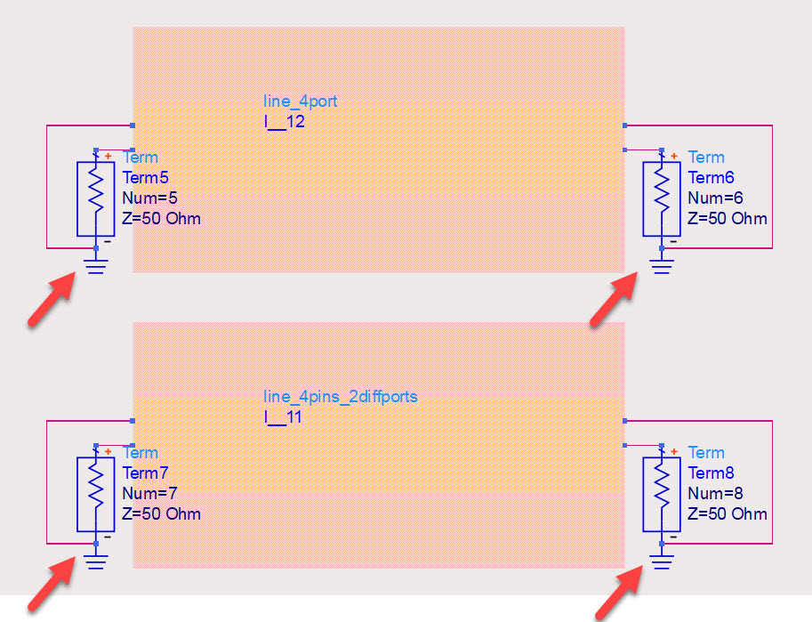
Now let’s create “bad and confusing” textbench, where we add schematic ground to the ground node of both ADS ports. What does that do? Is current through the ground conductor now “shorted” by that direct schematic ground connection?
To make the difference more visible, we used a very lossy material for the conductors: there is 10 ohm conductor resistance in the signal path on cond, and 4 ohm conductor resistance in the ground path on cond2.
For the line simulation with 2 differential ports (S87), adding those ground symbol gives the same transmission results as before. But for the line model simulated with 4 independent ports (S65), we have indeed created an ideal connection across the return path, resulting in a lower insertion loss. This is obviously wrong!
What does this mean for practical use? The 2-port model (result) with differential ports is “immune” to non-differential currents, and all current that flows into the signal conductor will return through the return path, no matter what else we try at schematic level. This is consistent with the explanation in the little theory chapter above. There is no risk of creating a “wrong” mode (or unphysical connection) by placing circuit grounds. But we cannot test conductors separately. Good or bad – you choose!
For the 4-port data, we can access both signal and return conductor separately. So the 4-port model with 4 independent ports, all using global ground reference, is the more universal solution. It allows to model both differential and common mode behaviour of the line. It also enables us to probe each conductor differently. The price to pay: it requires careful thought about ground connection at schematic level, so that we don’t accidentally create an ideal connection somewhere that bypasses parts of the line.


