This document describes the design and simulation of simple PCB antennas for 2.4GHz and 5.6GHz.
- The first example shows a 2.45GHz single band antenna.
- The second example then shows a dual band version for 2.4GHz and 5.6GHz.
- Finally, we will investigate the sensitivity to PCB material tolerances.
For design and simulation, Microwave Office v11 with the Axiem EM simulator is used.
Getting started: Inverted F antenna for 2.4GHz
PIFA antenna shapes have become popular in mobile phones, with a metal bracket as the radiating element at some distance above the PCB. Here, we want to design a truly planar PCB antenna with no such extra bracket, so we use the PCB conductor layers to form an inverted F shape.
(click pictures to view full size)
The basic idea is similar to the PIFA: We have a radiator of 1/4 wavelength, with one end connected to the PCB ground plane. The radiator is tapped at some distance from the ground connection, to connect the feed. The tap position changes the resulting input impedance, and so does the distance between the radiator and the ground plane.
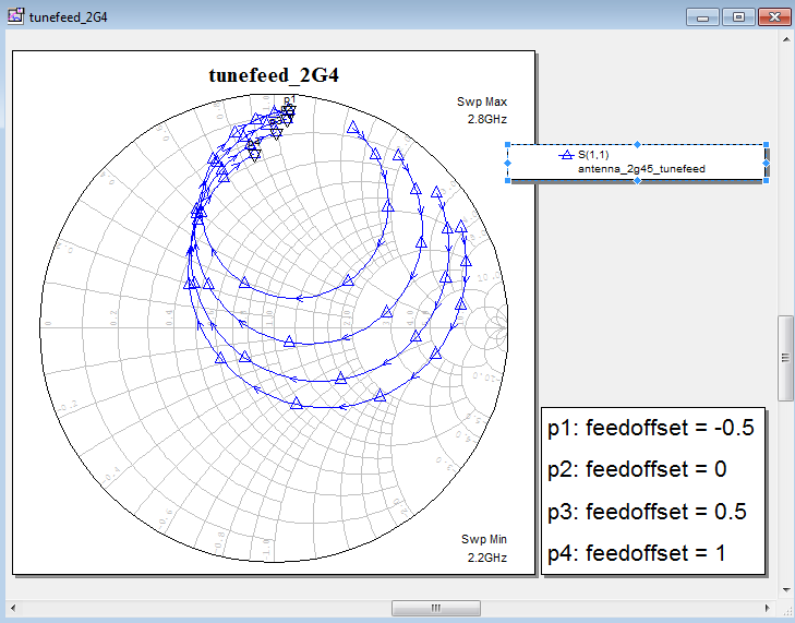
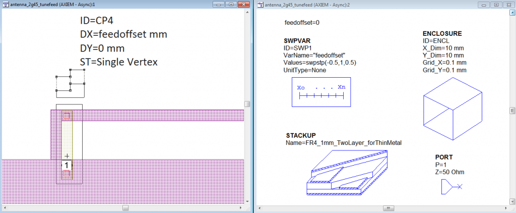
The plot below shows the antenna input impedance when the tap position is moved.
This parametric sweep was done by adding a Parametric Modifier of type Control Point and sweeping that control point with a variable in the EM schematic. It can be seen that in our case, the nominal value (feedoffset=0 mm) gives the closest match to 50 Ohm.
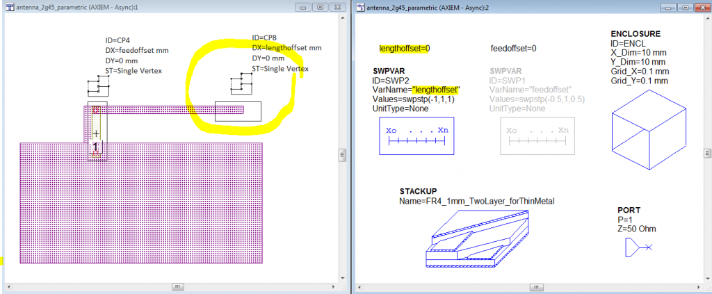
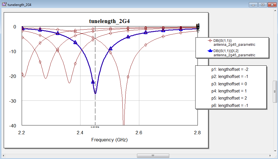
After determining the tap position for the feed, the antenna frequency can be fine tuned by adjusting the radiator length. There are multiple ways to define that length by parameters. Here, we have used a Parametric Modifier of type Control Point again.
With this sweep, we find that the antenna length must be tweaked by -1mm to reach the 2.45GHz target frequency. The matching changes only slightly for this small change in length, so we don’t need to re-tune the tap position again.
Now the antenna is tuned for good matching at 2.45GHz, but what about the antenna gain?
So far, we used the adaptive frequency sweep for EM simulations, which automatically chooses the EM analysis frequencies as needed, with only the start and stop frequency defined by the user. The adaptive frequency sweep gives us nicely interpolated S-parameters, but currents and antenna patterns are only available for the discrete frequencies that had actually been EM simulated. In Microwave Office these are called FSAMP frequencies.The screenshot below shows that we have 241 frequencies for S-parameters interpolated from 8 discrete EM analysis frequencies. Antenna patterns are only available for those 8 frequencies, which had been chosen automatically by the software. The nearest frequency to our 2.45GHz target is the 2.5GHz frequency point.
In our case, the antenna is matched narrowband and the internal losses change with frequency. For this reason, we want to simulate the antenna gain at the exact operating frequency. The easiest method is to create a copy of the EM structure and simulate that for a single frequency point 2.45GHz (no sweep, no AFS).
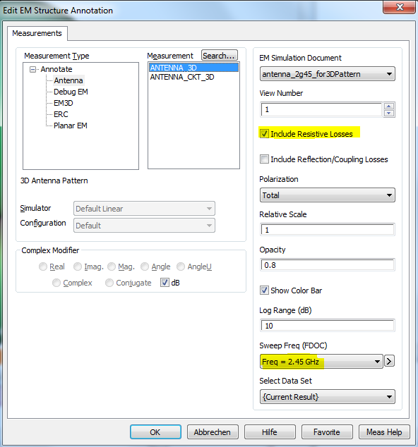
How to set the antenna annotation parameters for a 3D far field pattern? The screenshot below shows what settings you need to plot the antenna gain (dBi) with losses in the antenna included. If you disable the “Included Resistive Losses” checkbox you will get the antenna directivity instead of the gain.
The resulting pattern is shown below. The drop in radiation in the PCB plane isn’t real – this is an artefact from the MoM simulation method used by Axiem, which simulates with substrates of infinite size. These infinite substrates cause a drop in simulated gain at the horizon (theta=90°). The true pattern shape is continuous at the horizon, with no such drop.
The directivity (without losses) is around +2dBi peak. For the gain (including resistive losses) we get around 0dBi peak gain. This means that our antenna has reasonable efficiency, with approximately 2dB losses in conductors or dielectrics or both.
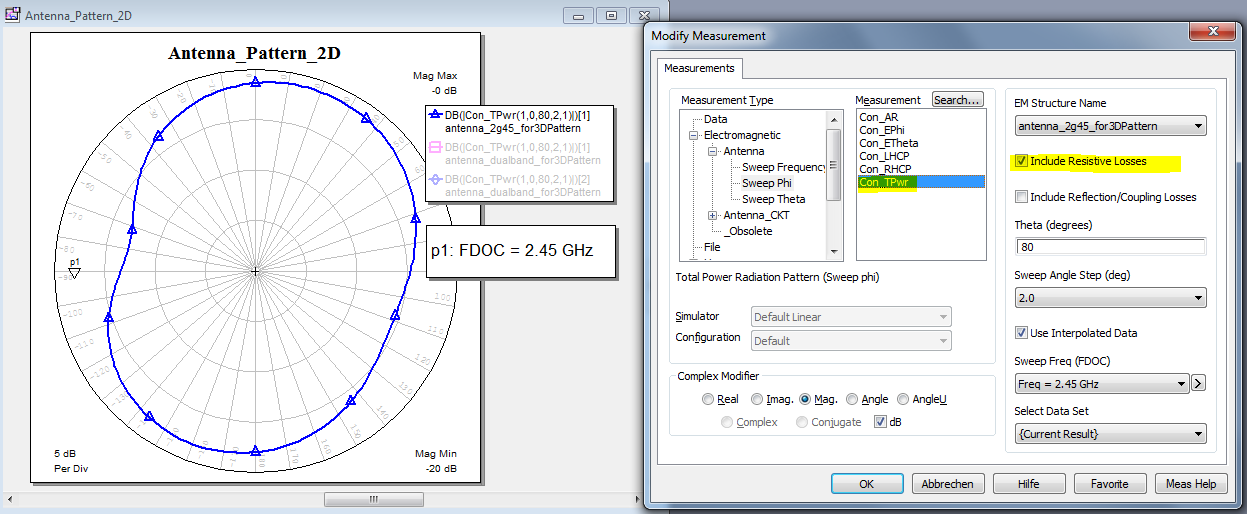
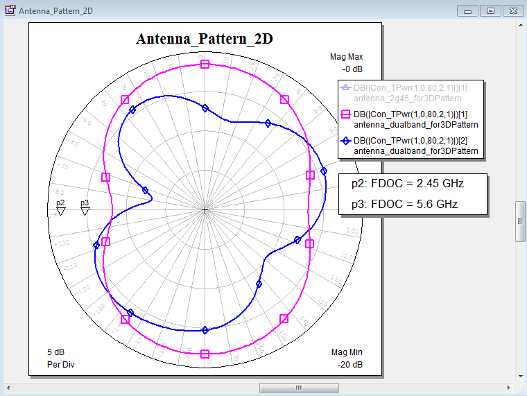
Besides the 3D pattern that gives a good overview of the radiation characteristics, we can also plot the “classical” antenna parameters in 2D polar format. Below is the result for the gain (total over all polarizations) at theta=80°, which is 10° above the PCB plane.
If the antenna had excessive losses, i.e. large difference between gain and directivity, we could now investigate the origin of these losses. This could be done by selectively setting only the metals or only the PCB dieelectric to lossless, to investigate what is causing the losses.
Extending the antenna to dualband: 2.45GHz and 5.6GHz
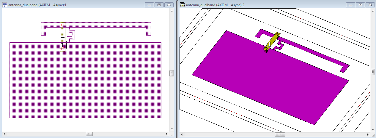
After investigating the simple single band antenna, we can now extend to to dual band operation at 2.45GHz and 5.6GHz. The layout is extended by adding a seconds radiator element.
We first match the antenna for 2.45GHz and set the 2.45Ghz length, then set the 5.6GHz length. The matching is now off, and in this case we find that we need more inductance between the feed tap and ground. This is achieved by adding a meander line instead of the straight line segment. Also, the tap location is moved again top find the best matching point for bother 2.45GHz and 5.6GHz. Finally, the lengths are fine tuned to the target frequencies.
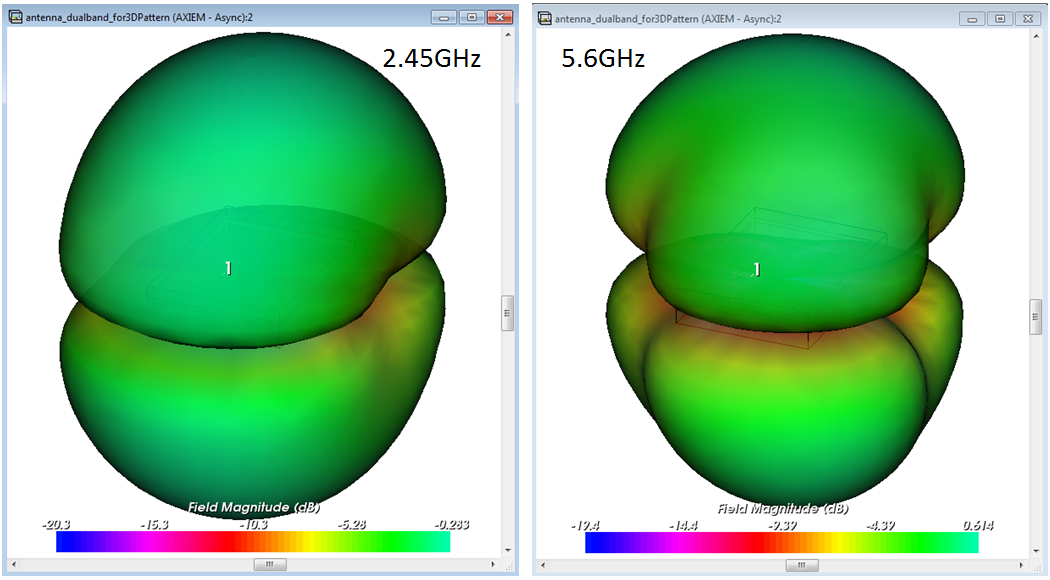
The 3D antenna gain annotation is calculated by copying the EM Structure and simulating that copy at 2 frequencies only: 2.45GHz and 5.6GHz (no sweep, no AFS).
It can be seen that the antenna performs reasonable, with around 0dBi peak gain. At 5.6GHz the pattern is more directed. The 2.4GHz performance is very similar to the single band version.
This almost completes our shout introduction on PCB F-antenna simulation in Microwave Office. But this topic wouldn’t be complete without a look at tolerances: the usual FR4 PCB material is poorly specified and large tolerances in permittivity must be expected.
Sensitivity to PCB material tolerances
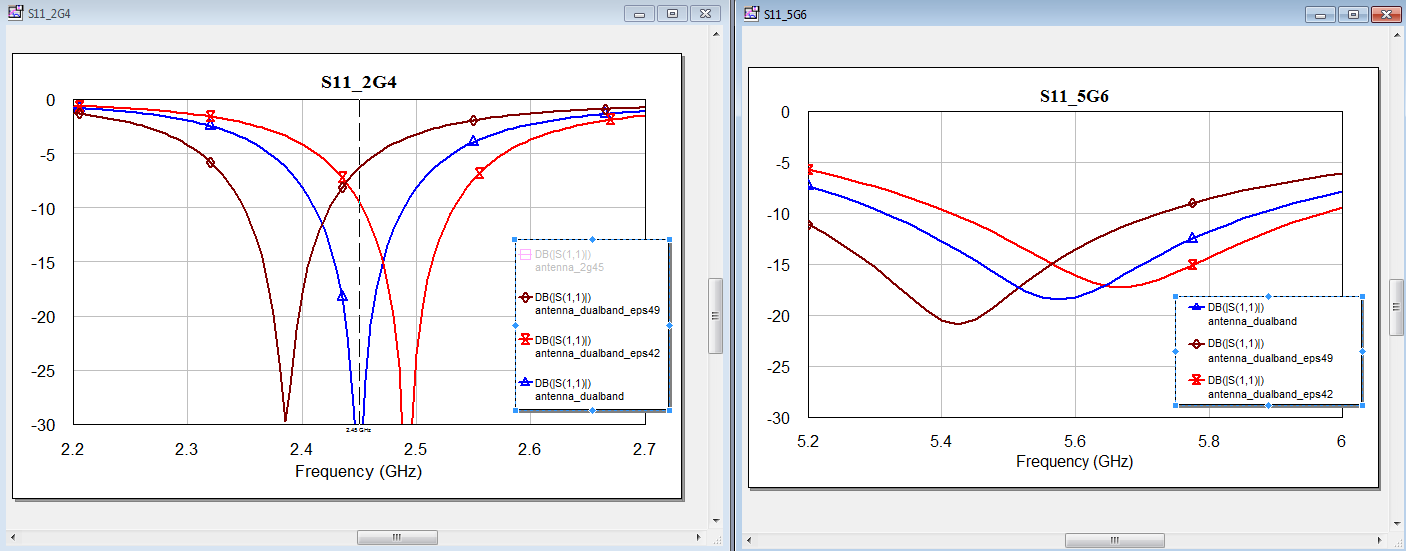
The final investigation on these antennas is the sensitivity to spread in FR4 dielectric properties. That value depends on the resin/fibre micture of the board material, and different manufacturers provide different materials. They all fall into that large “FR4” group, but it’s really different materials from an RF viewpoint. Reported values for FR4 dielectric constant are somewhere in the range 4.0 to 4.9. Simulations so far have been performed with a value of 4.47 as set in the MWO template for 2-layer FR4.
So how does the resonance shift when we simulate with er=4.2 and er=4.9 instead of 4.47? We copy and modify the dualband antenna, and this is what we get after re-simulating with the new values:
Now depending on our requirements, we can decide if this possible mismatch is acceptable, or if we want to go for an alternative PCB material with tighter tolerances.
Download of the Microwave Office example project:
antennas_2.45GHz_5.6GHz_muehlhaus.zip (59kB)
In part 2 of this application note, these advanced topics will be covered:
- Co-simulation of antenna and SMD matching components for electrically small antennas
- Using the Analyst 3D FEM solver to include the effect of finite PCB size, or possible PCB cutouts.
Keywords: WLAN antenna design, simulation, Antennensimulation, Antenne, Simulation, AWR MWO


