
[box type=warn]
Outdated! This application note was created for ADS 2012. In todays’s ADS version there is a built-in via merging feature that is more efficient than the methods described on this page!
[/box]
Via arrays
In RFIC, larger vias are created as via arrays. The size of each single via is usually fixed by the technology rules, and via arrays are created where a larger via cross section is needed. This application note describes efficient modelling of via arrays in Agilent ADS with the Momentum EM solver.

(click for full size)
Via arrays consist of many parallel conductors in z-direction, where no current can flow in the x-y plane. That’s a difference between via arrays and the solid via blocks (“via bar”, “slot via”) that are also available in some technologies: a solid via can also take horizontal current, but the via array can only take vertical current. This difference is important when metal layers are stacked with vias: the via array does not add cross section for the horizontal current flow, but a solid via does. Why do we care? Because that’s the behaviour of via arrays vs. solid vias in the real world, and we need to be carefuly with any via simplification that might change this current flow. This is discussed at the end of this application note.
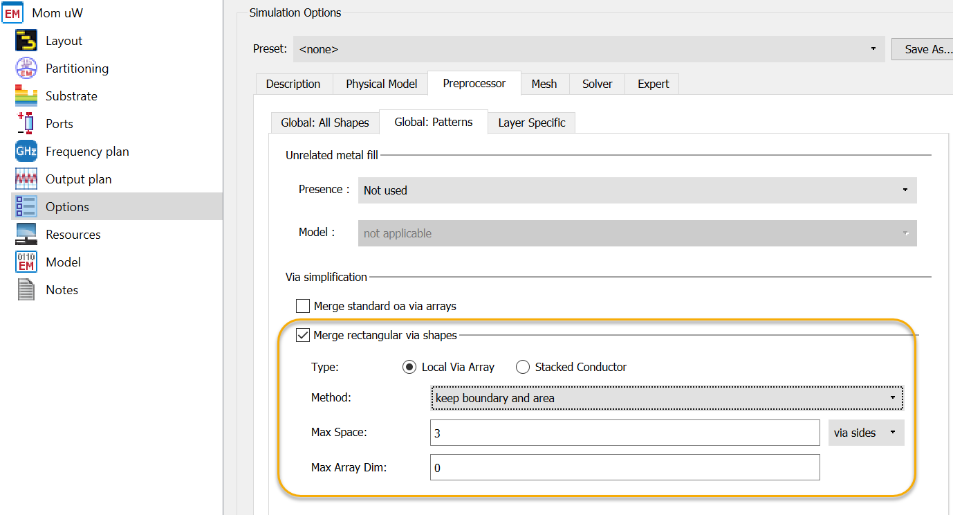
Via simplification by merging
Via simplification is usually done by combining the individual vias into a larger polygon that follows the outer boundary (or bounding box) of the via array. We will first discuss different ways how this merging can be done, and later deal with the errors and side effects of that approach.
Merging with an AEL script
The vias of an array can be merged by a series of oversize – merge – undersize commands: First, the size of each via is increased, until they overlap. Then, the overlapping shapes are merged, and finally the merged shape is undersized again, so that we get back to the original outline. This can be automated by an AEL script, as shown here:
[box]defun viamerge()
{
decl context = de_get_current_design_context();
// select everything on via layers
decl layerId = db_find_layerid_by_name(context,”contact:drawing”);
db_select_all_on_layerid(context, layerId, TRUE);
layerId = db_find_layerid_by_name(context,”via1:drawing”);
db_select_all_on_layerid(context, layerId, TRUE);
layerId = db_find_layerid_by_name(context,”via2:drawing”);
db_select_all_on_layerid(context, layerId, TRUE);
// oversize by 2 microns
de_set_oversize(2, 0);
de_oversize(1);
// combine shapes
de_union();
// undersize by 2 microns
de_set_oversize(-2, 0);
de_oversize(1);
de_deselect_all();
context = NULL;
}[/box]
The script is placed in the workspace directory, loaded from the ADS main windows and applied to a layout from the ADS command line. Obviously, the script needs to be adjusted for different via sizes and layer names.

(click for full size)
Implemented as above, the script is destructive: It replaces the via array by the merged shape, on the same layer.
Diagonal stepped vias create a staircase boundary. Vias with a spacing larger than the oversize value are not merged.

(click for full size)
What values should we use for oversize/undersize? Depending on the foundry and PDK implementation, there are subtle differences how Pcells generate via arrays with a given target size that doesn’t match exactly with n*viasize + (n-1)*viaspacing. The viasize or viaspacing might be slightly increased to match the total dimension. This is relevant for via simplification algorithms that are based on exact viasize and viaspacing values: better add some tolerance to handle these cases, i.e. used larger values for oversize/undersize, within reasonable limits. Too large values might create false connections (short circuit) between adjacent via arrays.
Via simplification by ADS 2012 derived layers
In ADS 2012.08, Agilent introduced the derived layer function “grow envelope” that we can use for via merging. But before we look at the actual implementation, let’s review the derived layer concept.
[pullquote align=right]If derived layers are not preconfigured in the PDK, no problem: The user can add them to his library where he has read/write access. [/pullquote] Derived layers is a new concept for layout preprocessing for EM which was introduced in ADS2011. Each derived layer takes some input information from one or more source layers, and performs some operations on the shapes found on these layers. This can be boolean operations or sizing, for example. The resulting new shapes are then written to the derived layer, without touching the original shapes on the source layers. So this is non-destructive, whereas our AEL-based via merging above was destructive and replaced the via arrays with the merged shapes. Besides beeing non-distructive, the “grow envelope” method also creates nicer diagonal shapes instead of the staircase pattern shown above.
Grow envope is new in ADS 2012.08. The only input parameters are the source layer and the desired growth. The word growth is misleading here, because the final shape has the correct boundary size and does not grow. Growth is only a temporary step for merging the shapes.

(click for full size)
What values should we use for growth? Depending on the foundry and PDK implementation, there are subtle differences how Pcells generate via arrays with a given target size that doesn’t match exactly with n*viasize + (n-1)*viaspacing. The viasize or viaspacing might be slightly increased to match the total dimension. This is relevant for via simplification algorithms that are based on exact viasize and viaspacing values: better add some tolerance to handle these cases, i.e. used larger values for oversize/undersize, within reasonable limits. Too large values might create false connections (short circuit) between adjacent via arrays.
[pullquote align=right]Derived layers are only visible to the EM simulator. You can see them in 3D EM preview, but not in the layout editor![/pullquote]How to check the outcome of the derived layer operation?
If you look at the layout editor, you will only see the original geometries, but no shapes from derived layers. Derived layers are only visible to the EM simulator, and shapes on derived layers are only created during the pre-processing phase of an EM simulation.
To actually use the shapes from the derived layers, map the derived layer in your EM substrate instead of the original source layer. That’s all you need to do.
Note that creating the derived layer shapes is a preprocessing step that must be enabled in the Preprocessing options (enabled by default). You can also force an update of the derived layer content without running the full simulation: at the bottom right of the emSetup dialog, you can choose what you want to generate. By default, that is set to “S-parameters”, but you could set it to “Pre-processed geometries” to run that step only. Only if you do this, then you will see the derived shapes in the layout editor.

(click for full size)
Now that we understand derived layers, we can apply this to via merging. The “grow envelope” function is perfect to calculate the via array’s boundary, and the resulting shapes on the derived layer can be mapped in the EM substrate instead of the original via geometries. The EM preview will then show the merged via boundary if things are configured properly (and if the via array is not merged properly, it will take forever to visualize the 3D model with thousands of individual vias …)

(click for full size)
Simulation accuracy: Side effects on via loss and Q factor
The big question is: the simulation is much faster with merged vias, but how accurate is it? There are different aspects that need to be considered.
Direction of current flow
In the beginning of this application note, we had discussed the different current flow in via arrays (vertical current only) versus solid via blocks (current can flow in any direction). By merging the via array into one solid via, we have changed the possible current flow from vertical (z-axis) to arbitrary (x,y,z). This is not a big deal for vias as shown above, but it does matter for wide via arrays in stacked conductor configurations.

(click for full size)
The original via array with its z-only current does not carry horizontal (x-y) current, so that the effective cross section of stacked metals is defined by the metal itself. If we now merge this via array to a solid via block, this changes the effective cross section of the line, by adding the via metal as an additional parallel conductor that can carry horizontal current. This is where the Momentum setting for via currents (2-D distributed or 3-D distributed) becomes relevant.

(click for full size)
By default, that setting defaults to 3-D distributed, which means that vias can carry current in all directions, including horizontal (x-y) currents. Again: we don’t wory much about small via arrays, but for large via arrays in stacked metal configurations, you want to set this to 2-D distributed if the true shape of that vias is an array. This prevents x-y current on the via that does not physically exist in the manufactured hardware. In case of doubt, double check with a simple testcase to see the effect.
Note that this settings will affect all vias in the simulation model. You could also make a choice per layer, but you can not change this setting per polygon.
If the physical via in the hardware is a solid block (“via bar”, “slot via”) that can carry horizontal current, then 3-D distributed is the correct choice. These solid vias are quite rare, but they exist in some RF-optimized technologies. They are typically on other layers than the via arrays, so that the per-layer setting for 2-D/3-D can be applied.
Effective size/cross section of the via
Another obvious effect of via merging is that we change the effective conductor cross section of the via: we now have the boundary fully filled with metal, where the original array was only partially filled with metal. The typical “fill factor” of an array is around 25%. By merging the vias into one solid block, we now have 100% fill factor. This reduces the via resistance in z-direction. [pullquote align=right]Our license agreement with Agilent does not permit to perform and publish benchmarks, so you need to run testcases yourself, if you want to be very accurate on via loss modelling.[/pullquote]
If we are interested only in the correct DC resistance, we could compensate for that error by lowering the conductivity. This is what Sonnet’s via merging internally does. However, due to skin effect, the current pushes to the outside vias, away from the inner part of the via (array). Skin effect depends on conductivity, and compensating an incorrect fill factor with a change in conductivity will then change skin effect and so on … Not obvious what the best approach would be.In most cases, the contribution from via resistance is really small, and most conductor loss is from the planar metals anyway. But in case of doubt, just set up a few simple test cases.