In part one of this application note we looked at basic design concepts and simulation methods for “printed” PCB antennas. Now in this second part, these advanced topics are discussed:
- Co-simulation of antenna and SMD matching components for electrically small antennas
- Using the Analyst 3D FEM solver to include the effect of finite PCB size, or possible PCB cutouts.
For design and simulation, Microwave Office v11 with the Axiem and Analyst EM simulators is used. The 868MHz antenna design in this example was created by consultant Lutz Konstroffer and is used with permission.
Axiem simulation (planar, infinite PCB)
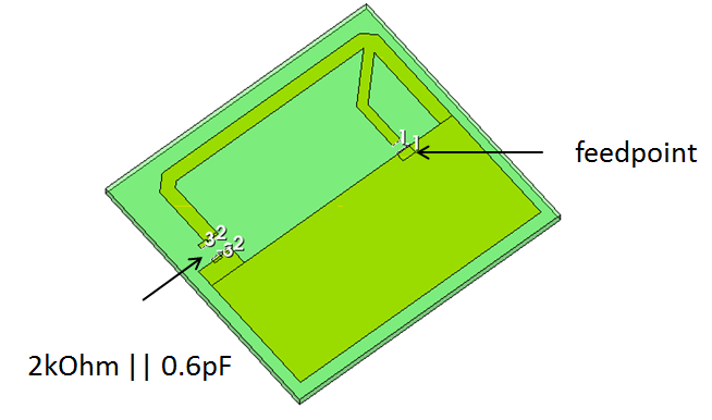
Let’s get started with the Axiem simulation of this antenna. After importing the layout from an artwork file, it is copied to a new EM structure. The design goal had been to design a small omnidirectional antenna for a handheld device that is insensitive to its environment. This was achieved by shortening the radiator with a capacitive top load, and placing a resistor in parallel to that top load. The resistor causes a lower gain, but that gain is now rather stable over different environments (different placement of the device in the user’s hand).
(click to see full size)
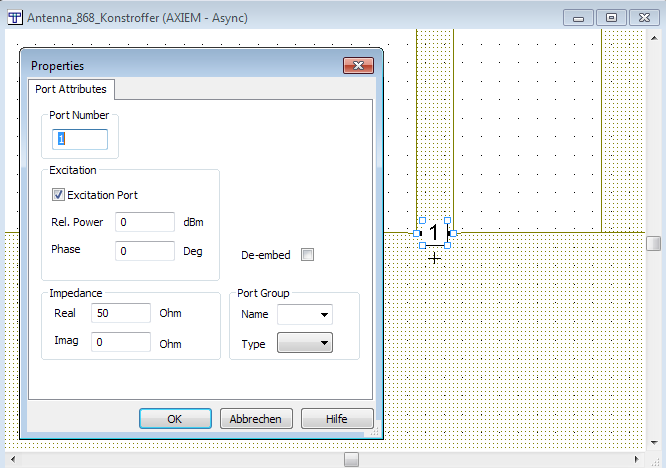
For the antenna input, an internal series port is added between the feedline and ground metal. This internally creates an infinitesimal gap with the (+) terminal on one side and the (-) terminal on the other side of the gap. It is equivalent to using explicit (+) and (-) pins over a gap, with the gap size shrinking to zero.
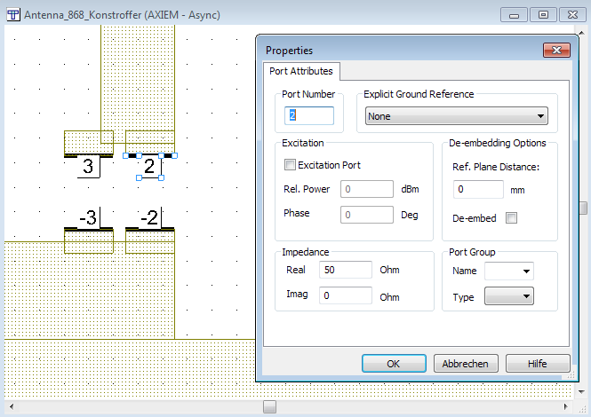
For the two SMD elements, explicit (+) and (-) pins are placed on the pads. This creates on differential port for each of the SMD elements.
The ports have explicit ground reference pins because there is no infinite ground in this model. Unlike a microstrip circuit, this antenna PCB has air above and below (no metal cover below substrate). Like all dielectric layers in Axiem, the FR4 dielectric for the PCB is modelled with infinite size in the x-y plane. We will come back to that later.
Now this EM structure can be simulated and we get 3-port S-parameter results. To get the comnined result for the antenna with matching network, we need to connect the SMD elements at ports 2 and 3. The schematic might look strange with the SMD connected to ground on one side, but that only means: connect these impedances between the (+) and (-) terminals of the corresponding ports. And because we have drawn explicit (-) terminals for these ports, that is where these “grounds” are connected.
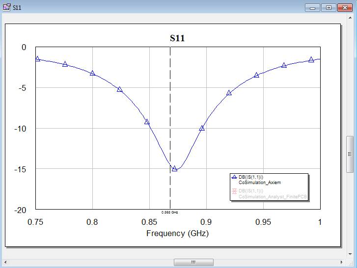
Now we can simulate the return loss of the antenna with the SMDs connected. Straighforward and simple. Please don’t worry about the nonlinear port definition shown above: for S-parameter simulation, it would also work with a normal linear port.
We can see that the antenna is matched, but what about the radiation pattern? That’s where it gets a bit tricky: that radiation pattern changes when we connect the SMD, so we must use EM-circuit co-simulation to get the corrrect radiation pattern. MWO can easily do that, as described below.
Co-Simulation to get the antenna pattern with SMD elements
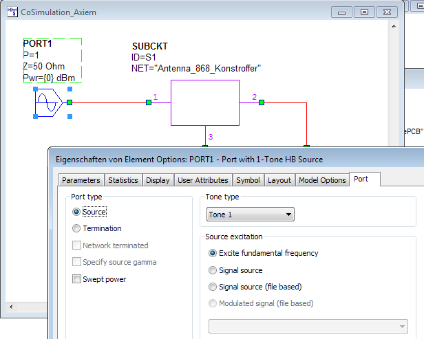
The 2D and 3D antenna patterns are calculated with special antenna annotations that reference both EM structure and a circuit simulation. After the EM simulation is finished, the circuit simulation calculates voltages and currents at the ports, and then uses this information to calculate the currents and far field of the antenna. As you might have guessed from the words “voltage” and “currents”, MWO wants us to run a non-linear Harmonic Balance simulation, even though our specific circuit doesn’t have non-linear devices.
So that’s why the schematic above was set up for non-linear simulation: to generate voltage/current data for co-simulated antenna patterns.
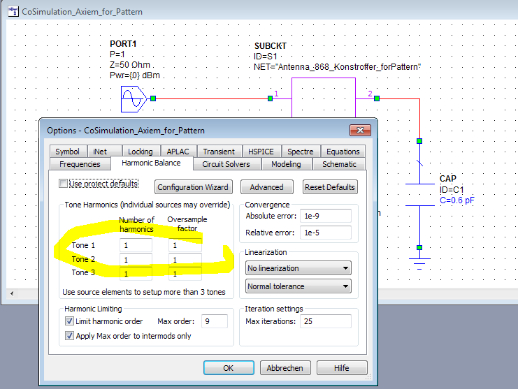
We are interested in that 868MHz fundamental frequency only. To avoid warnings from Harmonic Balance about missing EM results at n*868MHz harmonic frequency, we can set the number of harmonics to 1 in the co-simulation project settings. Alternatively, we could leave the defaults and just ignore warnings about extrapolation of EM results to harmonic frequencies.
Once we have this, we can create the annotation to visualize the co-simulated 3D antenna pattern. For simplicity, we can use a copy of the EM structure that is configured for single frequency 868MHz (so that we have EM results for that exact frequency) and a schematic that simulates that exact frequency.
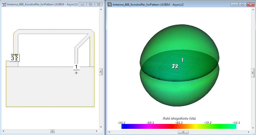
After simulating the schematic and EM structure, the 3D antenna pattern can be visualized.
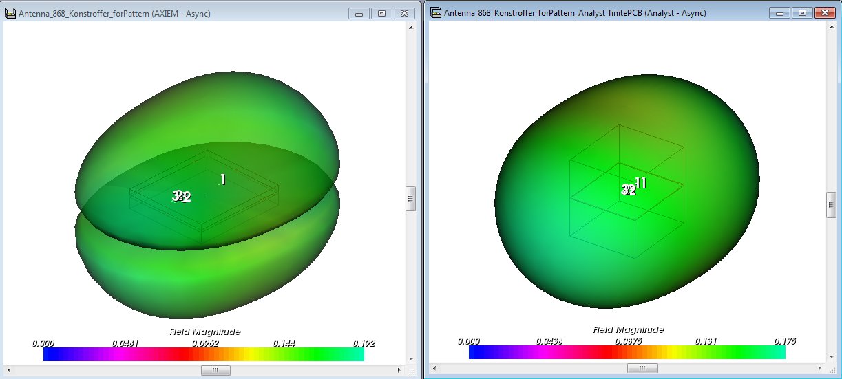
The drop in radiation in the PCB plane isn’t real – this is an artefact from the MoM simulation method used by Axiem, which simulates with substrates of infinite size. These infinite substrates cause a drop in simulated gain at the horizon (theta=90°). The true pattern shape is continuous at the horizon, with no such drop.
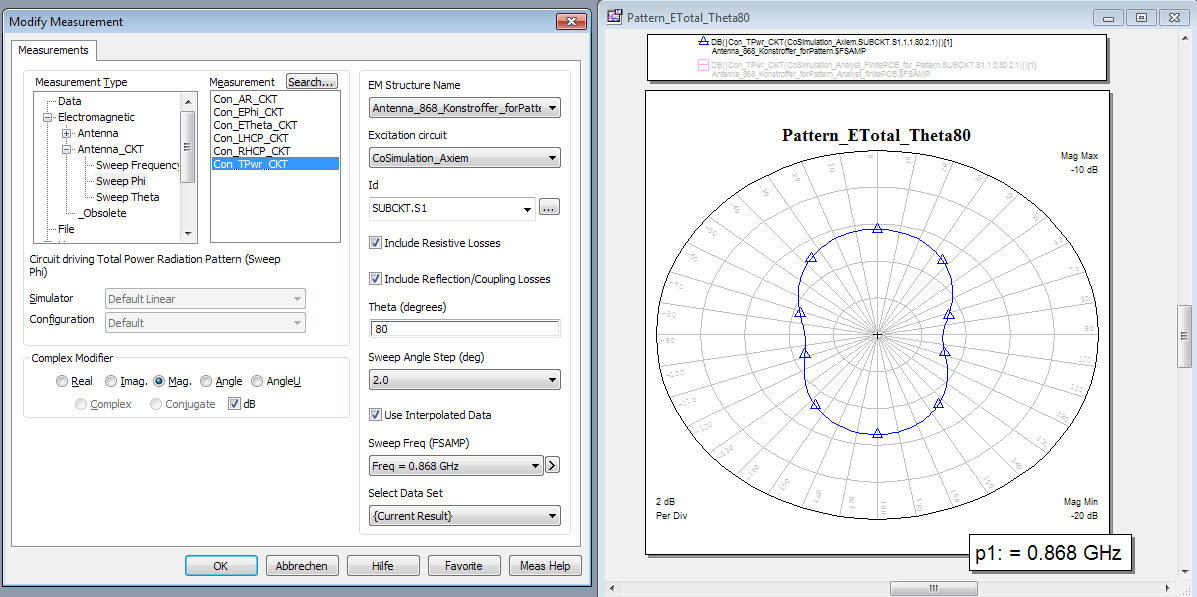
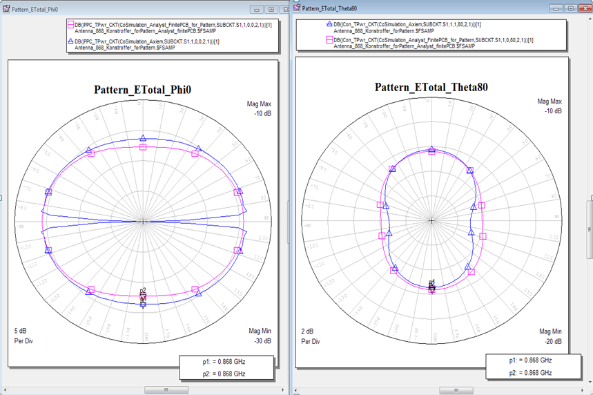
The antenna peak gain is around -14dBi with a really nice omni-directional antenna shape. Besides the 3D pattern that gives a good overview of the radiation characteristics, we can also plot the “classical” antenna parameters in 2D polar format. Below is the result for the gain (total over all polarizations) at theta=80°, which is 10° above the PCB plane.
The math of the Axiem solver that we used assumes that all dielectrics have infinite size. However, the real PCB size is limited. What effect does that have?
Include the finite PCB size – Analyst EM simulation
In Axiem we have simulated with an infinite PCB dielectric size. In reality, the PCB size is limited. There is a PCB edge near the antenna where the permittivity changes from 4.5 (FR4) to 1.0 (air). From that, we would expect that the measured antenna resonance frequency is slightly above the resonance that we simulated with Axiem (infinite dielectrics).
With the Analyst 3D FEM solver, we can include the finite PCB size in simulation. The price to pay, besides the license cost: Analyst solves a more general problem which takes more time and usually more memory. We want to avoid that heavy 3D simulation if Axiem and the infinite substrate assumption are good enough, but let’s do the comparison now for the PCB antenna.
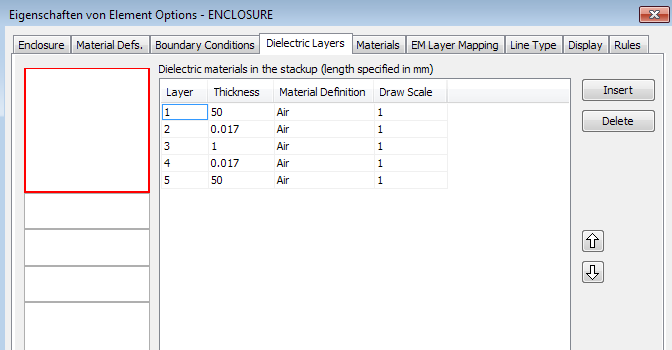
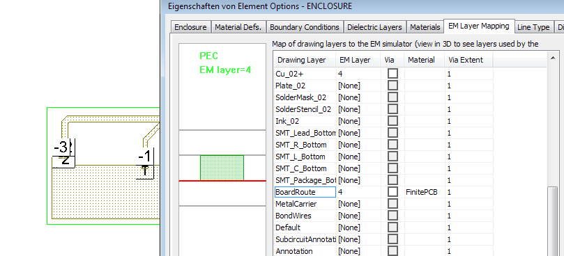
The EM stackup is modified for the finite substrate calculation: the infinite FR4 dielectric is changed to air, and FR4 is only selectively inserted by drawing a PCB rectangle that is properly mapped:
We create a material definition named “FinitePCB” with 1mm thickness and material FR4…
.. map it in the PCB location and assign it to drawing layer “BoardRoute”.
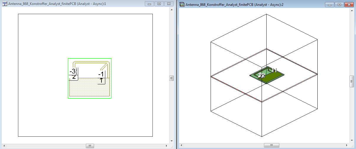
There is no special meaning in using that drawing layer, we could use any other layer that isn’t used otherwise. Now by drawing on that layer “BoardRoute”, we create a finite size FR4 dielectric for the PCB.
The simulation boundaries (sidewalls as well as top/bottom) are placed at a minimum distance of ~ 1/4 wavelength.
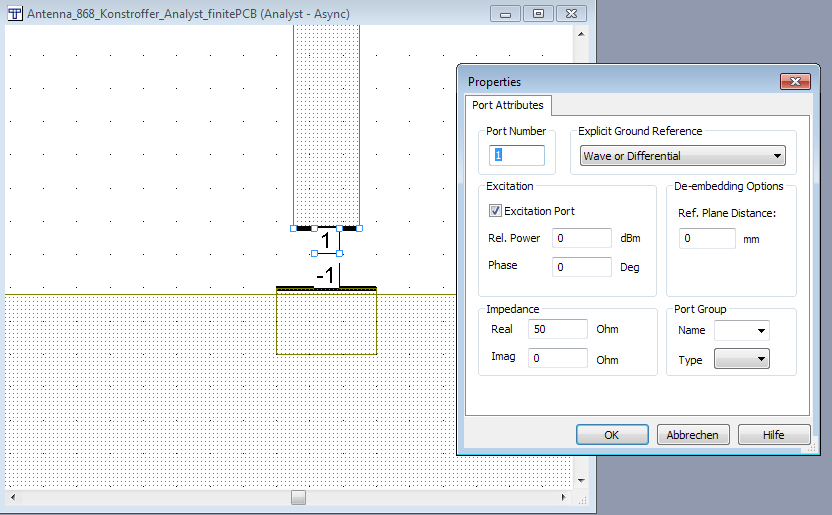
One final change that we need to make: Analyst doesn’t support the internal port that we used for Axiem, so we have to change that to a differential port with separate (+) and (-) pins.
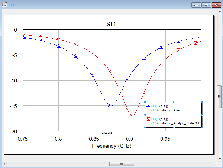
After making that change, we can simulate the EM model. The schematic for connecting the SMD is similar to the Axiem schematic shown earlier in this application note. After running that simualtion, we can compare the S11 results for Axiem (infinite PCB) and Analyst (finite PCB):
The result is what we intuitively expected: with the finite PCB size, the effective dielectric constant is slightly smaller and the antenna resonance goes up. However, the effect isn’t too bad and we can compensate that easily by tweaking the series capacitor value. This tweak is pure circuit simulation, so we don’t need to repeat the time consuming EM simulation.
What about the antenna pattern? Above we said that the drop in the gain at the horizon isn’t real, and only caused by Axiem’s infinite substrate. Let’s see what we get from the finite pattern simulation in Analyst, and how the patterns compare. Left is infinite substrate (Axiem) and right is finite substrate (Analyst). Plots are done with linear scale (not dB) for better comparison, because the present MWO release uses different auto-scaling rules for both solvers in the 3D viewer when using dB scale.
And finally the comparison of the 2D patterns. The antenna pattern and gain calculated by Axiem with the infinite substrate is rather similar to the Analyst 3D FEM results, except for data at the horizon (theta=90°). Knowing that this drop at the horizon isn’t real for this antenna type, we can simply ignore it, and use Axiem for efficient and fast design of PCB antennas.
Download of the Microwave Office example project:
antenna_868MHz_Axiem_Analyst.zip (42kB)
Keywords: 868MHz 915MHz ISM antenna design, M2M communication antenna simulation, Antennensimulation, Antenne, Simulation, AWR MWO

